
Page 294 - A Practical Guide from Design Planning to Manufacturing
P. 294
264 Chapter Nine
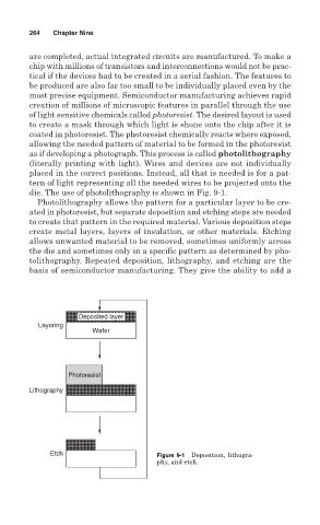
are completed, actual integrated circuits are manufactured. To make a
chip with millions of transistors and interconnections would not be prac-
tical if the devices had to be created in a serial fashion. The features to
be produced are also far too small to be individually placed even by the
most precise equipment. Semiconductor manufacturing achieves rapid
creation of millions of microscopic features in parallel through the use
of light sensitive chemicals called photoresist. The desired layout is used
to create a mask through which light is shone onto the chip after it is
coated in photoresist. The photoresist chemically reacts where exposed,
allowing the needed pattern of material to be formed in the photoresist
as if developing a photograph. This process is called photolithography
(literally printing with light). Wires and devices are not individually
placed in the correct positions. Instead, all that is needed is for a pat-
tern of light representing all the needed wires to be projected onto the
die. The use of photolithography is shown in Fig. 9-1.
Photolithography allows the pattern for a particular layer to be cre-
ated in photoresist, but separate deposition and etching steps are needed
to create that pattern in the required material. Various deposition steps
create metal layers, layers of insulation, or other materials. Etching
allows unwanted material to be removed, sometimes uniformly across
the die and sometimes only in a specific pattern as determined by pho-
tolithography. Repeated deposition, lithography, and etching are the
basis of semiconductor manufacturing. They give the ability to add a
Deposited layer
Layering
Wafer
Photoresist
Lithography
Etch Figure 9-1 Deposition, lithogra-
phy, and etch.