
Page 298 - A Practical Guide from Design Planning to Manufacturing
P. 298
268 Chapter Nine
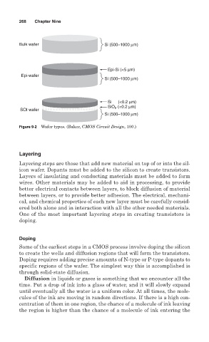
Bulk wafer Si (500–1000 µm)
Epi-Si (<5 µm)
Epi-wafer
Si (500–1000 µm)
Si (<0.2 µm)
(<0.2 µm)
SiO 2
SOI wafer
Si (500–1000 µm)
Figure 9-2 Wafer types. (Baker, CMOS Circuit Design, 100.)
Layering
Layering steps are those that add new material on top of or into the sil-
icon wafer. Dopants must be added to the silicon to create transistors.
Layers of insulating and conducting materials must be added to form
wires. Other materials may be added to aid in processing, to provide
better electrical contacts between layers, to block diffusion of material
between layers, or to provide better adhesion. The electrical, mechani-
cal, and chemical properties of each new layer must be carefully consid-
ered both alone and in interaction with all the other needed materials.
One of the most important layering steps in creating transistors is
doping.
Doping
Some of the earliest steps in a CMOS process involve doping the silicon
to create the wells and diffusion regions that will form the transistors.
Doping requires adding precise amounts of N-type or P-type dopants to
specific regions of the wafer. The simplest way this is accomplished is
through solid-state diffusion.
Diffusion in liquids or gases is something that we encounter all the
time. Put a drop of ink into a glass of water, and it will slowly expand
until eventually all the water is a uniform color. At all times, the mole-
cules of the ink are moving in random directions. If there is a high con-
centration of them in one region, the chance of a molecule of ink leaving
the region is higher than the chance of a molecule of ink entering the