
Page 300 - A Practical Guide from Design Planning to Manufacturing
P. 300
270 Chapter Nine
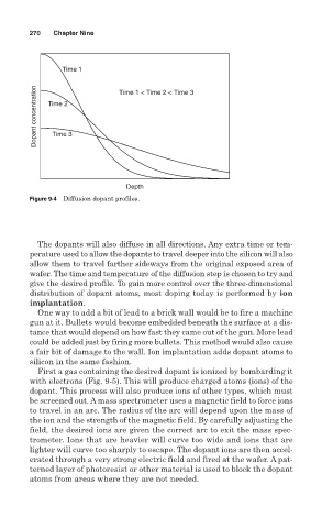
Time 1 Time 1 < Time 2 < Time 3
Dopant concentration Time 2
Time 3
Depth
Figure 9-4 Diffusion dopant profiles.
The dopants will also diffuse in all directions. Any extra time or tem-
perature used to allow the dopants to travel deeper into the silicon will also
allow them to travel farther sideways from the original exposed area of
wafer. The time and temperature of the diffusion step is chosen to try and
give the desired profile. To gain more control over the three-dimensional
distribution of dopant atoms, most doping today is performed by ion
implantation.
One way to add a bit of lead to a brick wall would be to fire a machine
gun at it. Bullets would become embedded beneath the surface at a dis-
tance that would depend on how fast they came out of the gun. More lead
could be added just by firing more bullets. This method would also cause
a fair bit of damage to the wall. Ion implantation adds dopant atoms to
silicon in the same fashion.
First a gas containing the desired dopant is ionized by bombarding it
with electrons (Fig. 9-5). This will produce charged atoms (ions) of the
dopant. This process will also produce ions of other types, which must
be screened out. A mass spectrometer uses a magnetic field to force ions
to travel in an arc. The radius of the arc will depend upon the mass of
the ion and the strength of the magnetic field. By carefully adjusting the
field, the desired ions are given the correct arc to exit the mass spec-
trometer. Ions that are heavier will curve too wide and ions that are
lighter will curve too sharply to escape. The dopant ions are then accel-
erated through a very strong electric field and fired at the wafer. A pat-
terned layer of photoresist or other material is used to block the dopant
atoms from areas where they are not needed.