
Page 304 - A Practical Guide from Design Planning to Manufacturing
P. 304
274 Chapter Nine
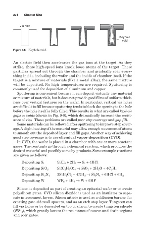
Via hole
Keyhole
void
Figure 9-8 Keyhole void.
An electric field then accelerates the gas ions at the target. As they
strike, these high-speed ions knock loose atoms of the target. These
particles spread out through the chamber and gradually coat every-
thing inside, including the wafer and the inside of chamber itself. If the
target is a mixture of materials (like a metal alloy), the same mixture
will be deposited. No high temperatures are required. Sputtering is
commonly used for deposition of aluminum and copper.
Sputtering is convenient because it can deposit virtually any material
or mixture of materials, but it does not provide good films of uniform thick-
ness over vertical features on the wafer. In particular, vertical via holes
are difficult to fill because sputtering tends to block the opening to the hole
before the hole itself is fully filled. This results in what are called keyhole
gaps or voids (shown in Fig. 9-8), which dramatically increase the resist-
ance of vias. These problems are called poor step coverage and gap fill.
Some materials can be reflowed after sputtering to improve step cover-
age. Aslight heating of the material may allow enough movement of atoms
to smooth out the deposited layer and fill gaps. Another way of achieving
good step coverage is to use chemical vapor deposition (CVD).
In CVD, the wafer is placed in a chamber with one or more reactant
gases. The reactants go through a chemical reaction, which produces the
desired material and possibly some by-products. Some example reactions
are given as follows:
Depositing Si SiCl + 2H → Si + 4HCl
2
4
Si(C H O) → SiO + 2H O + 4C H
Depositing SiO 2 2 5 4 2 2 2 4
Depositing Si N 4 3SiH Cl + 4NH → Si N + 6HCl + 6H 2
3
3
3
4
2
2
Depositing W WF + 3H → W + 6HF
2
6
Silicon is deposited as part of creating an epitaxial wafer or to create
polysilicon gates. CVD silicon dioxide is used as an insulator to sepa-
rate interconnect layers. Silicon nitride is used as a diffusion barrier, for
creating gate sidewall spacers, and as an etch stop layer. Tungsten can
fill via holes or be deposited on top of silicon to create tungsten silicide
), which greatly lowers the resistance of source and drain regions
(WSi 2
and poly gates.