
Page 306 - A Practical Guide from Design Planning to Manufacturing
P. 306
276 Chapter Nine
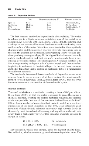
TABLE 9-1 Deposition Methods
Cost Step coverage & gap fill Common materials
Spin-on Low Good Photoresist, SiO 2
Sputtering Medium Poor Al, Cu, alloys
CVD High Good Si, SiO 2 , Si 3 N 4 , W
Electroplating Low Good Cu, Pb, Sn
The last common method for deposition is electroplating. The wafer
is submerged in a liquid solution containing ions of the metal to be
deposited. An electrode of the same metal is placed in the solution and
a voltage source connected between the electrode and a conducting layer
on the surface of the wafer. Metal ions are attracted to the negatively
charged wafer, and the positively charged electrode emits more ions as
those in the solution are deposited. Electroplating is low cost and pro-
vides good step coverage and gap fill. Its biggest limitations are that only
metals can be deposited and that the wafer must already have a con-
ducting layer on its surface to be electroplated. A common solution is to
first use sputtering to deposit a thin layer of metal, and then use elec-
troplating to add metal to this initial layer. In the end, there is no one
method of deposition that is best for all materials. Table 9-1 summarizes
the different methods.
The trade-offs between different methods of deposition cause most
process flows to use a mixture of all four, picking the most suitable
method for each individual layer. A special form of CVD that deserves
its own discussion is the creation of thermal oxide layers.
Thermal oxidation
Thermal oxidation is a method of creating a layer of SiO on silicon.
2
It is a form of CVD in that the wafer is exposed to gases that cause a
chemical reaction, creating the desired material. What makes thermal
oxidation special is that one of the reactants is the silicon wafer itself.
Silicon has a number of properties that make it useful as a semicon-
ductor; one of the most important is that SiO is an extremely good
2
insulator. Silicon dioxide tolerates extremely high electric fields, is
chemically inert, is mechanically strong, and any silicon wafer will nat-
urally form a high-quality layer of this insulator if simply exposed to
oxygen or steam.
Si + O → SiO 2 Dry oxidation
2
Wet oxidation
Si + 2H 2 O → SiO 2 + 2H 2
Dry oxidation, which uses oxygen, gives the highest quality films.
Wet oxidation, which uses steam, gives the fastest deposition rates. The