
Page 311 - A Practical Guide from Design Planning to Manufacturing
P. 311
Semiconductor Manufacturing 281
Photoresist
Spin-on Chrome
and
soft bake
Quartz
E-beam
Write
and Chrome
develop and
hard bake Quartz
Etch
and
strip Quartz
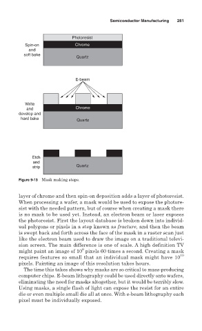
Figure 9-13 Mask making steps.
layer of chrome and then spin-on deposition adds a layer of photoresist.
When processing a wafer, a mask would be used to expose the photore-
sist with the needed pattern, but of course when creating a mask there
is no mask to be used yet. Instead, an electron beam or laser exposes
the photoresist. First the layout database is broken down into individ-
ual polygons or pixels in a step known as fracture, and then the beam
is swept back and forth across the face of the mask in a raster scan just
like the electron beam used to draw the image on a traditional televi-
sion screen. The main difference is one of scale. A high definition TV
6
might paint an image of 10 pixels 60 times a second. Creating a mask
requires features so small that an individual mask might have 10 10
pixels. Painting an image of this resolution takes hours.
The time this takes shows why masks are so critical to mass-producing
computer chips. E-beam lithography could be used directly onto wafers,
eliminating the need for masks altogether, but it would be terribly slow.
Using masks, a single flash of light can expose the resist for an entire
die or even multiple small die all at once. With e-beam lithography each
pixel must be individually exposed.