
Page 313 - A Practical Guide from Design Planning to Manufacturing
P. 313
Semiconductor Manufacturing 283
3.00 µm
2.00 µm
1.50 µm
Feature size
1.00 µm 1.00 µm
0.60 µm
0.50 µm
0.436 µm
0.40 µm
0.365 µm
Lithography wavelength
0.35 µm
0.248 µm
0.25 µm 0.193 µm
0.18 µm
0.15 µm 0.11 µm
0.13 µm
0.10 µm
1980 1984 1988 1992 1996 2000 2004
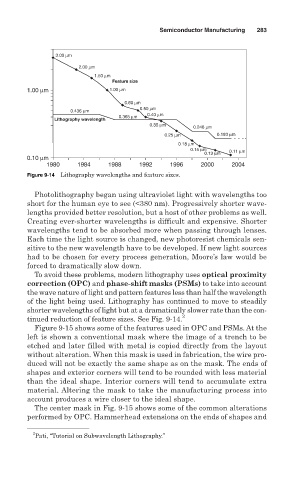
Figure 9-14 Lithography wavelengths and feature sizes.
Photolithography began using ultraviolet light with wavelengths too
short for the human eye to see (<380 nm). Progressively shorter wave-
lengths provided better resolution, but a host of other problems as well.
Creating ever-shorter wavelengths is difficult and expensive. Shorter
wavelengths tend to be absorbed more when passing through lenses.
Each time the light source is changed, new photoresist chemicals sen-
sitive to the new wavelength have to be developed. If new light sources
had to be chosen for every process generation, Moore’s law would be
forced to dramatically slow down.
To avoid these problems, modern lithography uses optical proximity
correction (OPC) and phase-shift masks (PSMs) to take into account
the wave nature of light and pattern features less than half the wavelength
of the light being used. Lithography has continued to move to steadily
shorter wavelengths of light but at a dramatically slower rate than the con-
tinued reduction of feature sizes. See Fig. 9-14. 2
Figure 9-15 shows some of the features used in OPC and PSMs. At the
left is shown a conventional mask where the image of a trench to be
etched and later filled with metal is copied directly from the layout
without alteration. When this mask is used in fabrication, the wire pro-
duced will not be exactly the same shape as on the mask. The ends of
shapes and exterior corners will tend to be rounded with less material
than the ideal shape. Interior corners will tend to accumulate extra
material. Altering the mask to take the manufacturing process into
account produces a wire closer to the ideal shape.
The center mask in Fig. 9-15 shows some of the common alterations
performed by OPC. Hammerhead extensions on the ends of shapes and
2
Pati, “Tutorial on Subwavelength Lithography.”