
Page 309 - A Practical Guide from Design Planning to Manufacturing
P. 309
Semiconductor Manufacturing 279
interconnect layers. Today copper is the interconnect material of choice
and some chips have seven to eight interconnect layers. The develop-
ment of CMP was a critical part of these process improvements.
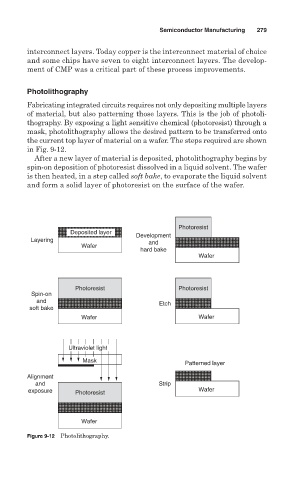
Photolithography
Fabricating integrated circuits requires not only depositing multiple layers
of material, but also patterning those layers. This is the job of photoli-
thography. By exposing a light sensitive chemical (photoresist) through a
mask, photolithography allows the desired pattern to be transferred onto
the current top layer of material on a wafer. The steps required are shown
in Fig. 9-12.
After a new layer of material is deposited, photolithography begins by
spin-on deposition of photoresist dissolved in a liquid solvent. The wafer
is then heated, in a step called soft bake, to evaporate the liquid solvent
and form a solid layer of photoresist on the surface of the wafer.
Photoresist
Deposited layer Development
Layering and
Wafer
hard bake
Wafer
Photoresist Photoresist
Spin-on
and Etch
soft bake
Wafer Wafer
Ultraviolet light
Mask
Patterned layer
Alignment
and Strip
exposure Photoresist Wafer
Wafer
Figure 9-12 Photolithography.