
Page 307 - A Practical Guide from Design Planning to Manufacturing
P. 307
Semiconductor Manufacturing 277
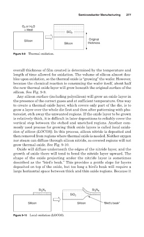
O or H O
2
2
+ Heat
SiO 2
Original
Silicon
Silicon thickness
Figure 9-9 Thermal oxidation.
overall thickness of film created is determined by the temperature and
length of time allowed for oxidation. The volume of silicon almost dou-
bles upon oxidation, so the thermal oxide is “growing” the wafer. However,
because the chemical reaction is consuming the wafer itself, about half
the new thermal oxide layer will grow beneath the original surface of the
silicon. See Fig. 9-9.
Any silicon surface (including polysilicon) will grow an oxide layer in
the presence of the correct gases and at sufficient temperature. One way
to create a thermal oxide layer, which covers only part of the die, is to
grow a layer over the whole die first and then after patterning with pho-
toresist, etch away the unwanted regions. If the oxide layer to be grown
is relatively thick, it is difficult in later depositions to reliably cover the
vertical step between the etched and unetched regions. Another com-
monly used process for growing thick oxide layers is called local oxida-
tion of silicon (LOCOS). In this process, silicon nitride is deposited and
then removed from regions where thermal oxide is needed. Neither oxygen
nor steam can diffuse through silicon nitride, so covered regions will not
grow thermal oxide. See Fig. 9-10.
Oxide will diffuse underneath the edges of the nitride layer, and the
growth of oxide there will tend to bend the nitride layer upward. The
shape of the oxide projecting under the nitride layer is sometimes
described as the “bird’s beak.” This provides a gentle slope for layers
deposited on top of the oxide, but too long a bird’s beak will require a
large horizontal space between thick and thin oxide regions. Because it
Si N Si N
3 4
3 4
SiO 2
Silicon Silicon “Bird's beak”
Figure 9-10 Local oxidation (LOCOS).