
Page 308 - A Practical Guide from Design Planning to Manufacturing
P. 308
278 Chapter Nine
allows the creation of extremely thin, very reliable oxide layers, ther-
mal oxide is the most common method for creating the gate oxide
between the polysilicon gate and the silicon channel. The ability to
easily create high-quality gate oxides is one of the most important factors
in the overall success of silicon MOSFETs in the marketplace.
Planarization
A common step after the addition of any material layer is planarization
to create a flat surface for the next processing step. This has become
more critical as more layers of material are used. Starting from a nearly
perfectly flat wafer, several layers of interconnect can make the surface
a tiny mountain range. Photolithography must focus the image being
patterned, but variation in the height of the wafer surface will blur this
image. Abrupt variations in height are also more difficult to reliably
cover in deposition steps. To prevent these problems from becoming
worse after each new layer, most processes use chemical-mechanical
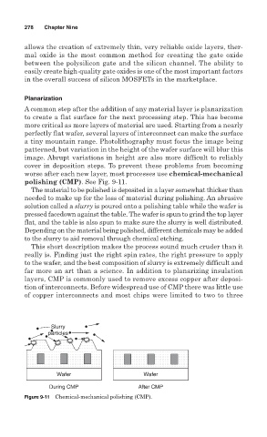
polishing (CMP). See Fig. 9-11.
The material to be polished is deposited in a layer somewhat thicker than
needed to make up for the loss of material during polishing. An abrasive
solution called a slurry is poured onto a polishing table while the wafer is
pressed facedown against the table. The wafer is spun to grind the top layer
flat, and the table is also spun to make sure the slurry is well distributed.
Depending on the material being polished, different chemicals may be added
to the slurry to aid removal through chemical etching.
This short description makes the process sound much cruder than it
really is. Finding just the right spin rates, the right pressure to apply
to the wafer, and the best composition of slurry is extremely difficult and
far more an art than a science. In addition to planarizing insulation
layers, CMP is commonly used to remove excess copper after deposi-
tion of interconnects. Before widespread use of CMP there was little use
of copper interconnects and most chips were limited to two to three
Slurry
particles
Wafer Wafer
During CMP After CMP
Figure 9-11 Chemical-mechanical polishing (CMP).