
Page 303 - A Practical Guide from Design Planning to Manufacturing
P. 303
Semiconductor Manufacturing 273
Target
E-field Ar + E-field
Wafer Wafer
Spin-on Sputtering
By-product
Reactant 1 Reactant 2 Electrode
±
Deposition Ions
Wafer Wafer
CVD Electroplating
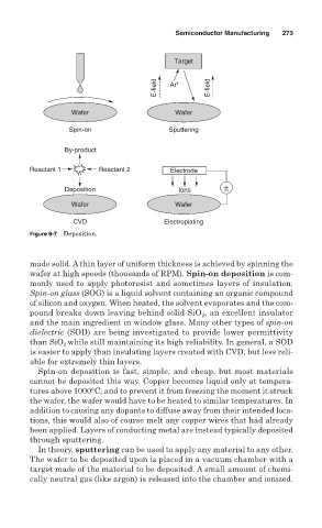
Figure 9-7 Deposition.
made solid. A thin layer of uniform thickness is achieved by spinning the
wafer at high speeds (thousands of RPM). Spin-on deposition is com-
monly used to apply photoresist and sometimes layers of insulation.
Spin-on glass (SOG) is a liquid solvent containing an organic compound
of silicon and oxygen. When heated, the solvent evaporates and the com-
pound breaks down leaving behind solid SiO , an excellent insulator
2
and the main ingredient in window glass. Many other types of spin-on
dielectric (SOD) are being investigated to provide lower permittivity
while still maintaining its high reliability. In general, a SOD
than SiO 2
is easier to apply than insulating layers created with CVD, but less reli-
able for extremely thin layers.
Spin-on deposition is fast, simple, and cheap, but most materials
cannot be deposited this way. Copper becomes liquid only at tempera-
tures above 1000°C, and to prevent it from freezing the moment it struck
the wafer, the wafer would have to be heated to similar temperatures. In
addition to causing any dopants to diffuse away from their intended loca-
tions, this would also of course melt any copper wires that had already
been applied. Layers of conducting metal are instead typically deposited
through sputtering.
In theory, sputtering can be used to apply any material to any other.
The wafer to be deposited upon is placed in a vacuum chamber with a
target made of the material to be deposited. A small amount of chemi-
cally neutral gas (like argon) is released into the chamber and ionized.