
Page 302 - A Practical Guide from Design Planning to Manufacturing
P. 302
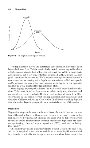
272   Chapter Nine


                     Implant 1


          Dopant concentration  Implant 2


                                Depth
        Figure 9-6 Ion implantation dopant profiles.


          Ion implantation allows the maximum concentration of dopants to be
        beneath the surface. This is particularly useful in creating wells where
        a high concentration is desirable at the bottom of the well to prevent leak-
        age currents, but a low concentration is needed at the surface to allow
        good transistor drive current. Wells created through implantation with
        concentration increasing with depth are sometimes called retrograde
        wells because the concentration changes with depth in the opposite
        manner as wells created through diffusion alone.
          After doping, any step that heats the wafers will cause further diffu-
        sion. This must be taken into account when designing the dose and
        energy of the initial implant. The final distribution of dopants will be
        determined by the parameters of the implant itself and the amount and
        duration of all future heating of the wafer. In addition to adding dopants
        into the wafer, layering steps add new materials on top of the wafer.

        Deposition
        Deposition steps add a new continuous layer of material across the sur-
        face of the wafer. Later, patterning and etching steps may remove mate-
        rial in selected regions, but initially the layer will be deposited across
        the entire wafer. The four most common methods of deposition are spin-
        on, sputtering, chemical vapor deposition (CVD), and electroplating.
        See Fig. 9-7.
          The easiest way to add a new material to a wafer is simply to pour it on.
        All that is required is that the material can be made liquid or dissolved
        in a liquid at a suitably low temperature and somehow later cured to be