
Page 297 - A Practical Guide from Design Planning to Manufacturing
P. 297
Semiconductor Manufacturing 267
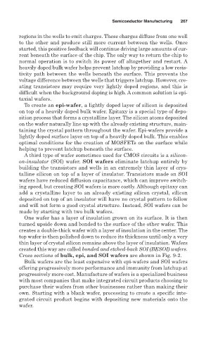
regions in the wells to emit charges. These charges diffuse from one well
to the other and produce still more current between the wells. Once
started, this positive feedback will continue driving large amounts of cur-
rent beneath the surface of the chip. The only way to return the chip to
normal operation is to switch its power off altogether and restart. A
heavily doped bulk wafer helps prevent latchup by providing a low resis-
tivity path between the wells beneath the surface. This prevents the
voltage difference between the wells that triggers latchup. However, cre-
ating transistors may require very lightly doped regions, and this is
difficult when the background doping is high. A common solution is epi-
taxial wafers.
To create an epi-wafer, a lightly doped layer of silicon is deposited
on top of a heavily doped bulk wafer. Epitaxy is a special type of depo-
sition process that forms a crystalline layer. The silicon atoms deposited
on the wafer naturally line up with the already existing structure, main-
taining the crystal pattern throughout the wafer. Epi-wafers provide a
lightly doped surface layer on top of a heavily doped bulk. This enables
optimal conditions for the creation of MOSFETs on the surface while
helping to prevent latchup beneath the surface.
A third type of wafer sometimes used for CMOS circuits is a silicon-
on-insulator (SOI) wafer. SOI wafers eliminate latchup entirely by
building the transistors and wells in an extremely thin layer of crys-
talline silicon on top of a layer of insulator. Transistors made on SOI
wafers have reduced diffusion capacitance, which can improve switch-
ing speed, but creating SOI wafers is more costly. Although epitaxy can
add a crystalline layer to an already existing silicon crystal, silicon
deposited on top of an insulator will have no crystal pattern to follow
and will not form a good crystal structure. Instead, SOI wafers can be
made by starting with two bulk wafers.
One wafer has a layer of insulation grown on its surface. It is then
turned upside down and bonded to the surface of the other wafer. This
creates a double-thick wafer with a layer of insulation in the center. The
top wafer is then polished down to reduce its thickness until only a very
thin layer of crystal silicon remains above the layer of insulation. Wafers
created this way are called bonded and etched-back SOI (BESOI) wafers.
Cross sections of bulk, epi, and SOI wafers are shown in Fig. 9-2.
Bulk wafers are the least expensive with epi-wafers and SOI wafers
offering progressively more performance and immunity from latchup at
progressively more cost. Manufacture of wafers is a specialized business
with most companies that make integrated circuit products choosing to
purchase their wafers from other businesses rather than making their
own. Starting with a blank wafer, processing to create a specific inte-
grated circuit product begins with depositing new materials onto the
wafer.