
Page 301 - A Practical Guide from Design Planning to Manufacturing
P. 301
Semiconductor Manufacturing 271
As + Mass
AsF gas spectrometer
5
and other ions
e −
Ion source As +
Acceleration
tube
As +
PR PR
N+
diffusion
region
Si wafer
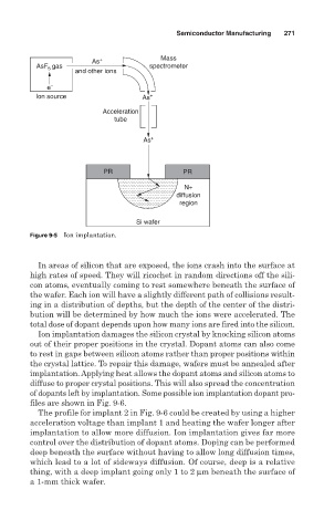
Figure 9-5 Ion implantation.
In areas of silicon that are exposed, the ions crash into the surface at
high rates of speed. They will ricochet in random directions off the sili-
con atoms, eventually coming to rest somewhere beneath the surface of
the wafer. Each ion will have a slightly different path of collisions result-
ing in a distribution of depths, but the depth of the center of the distri-
bution will be determined by how much the ions were accelerated. The
total dose of dopant depends upon how many ions are fired into the silicon.
Ion implantation damages the silicon crystal by knocking silicon atoms
out of their proper positions in the crystal. Dopant atoms can also come
to rest in gaps between silicon atoms rather than proper positions within
the crystal lattice. To repair this damage, wafers must be annealed after
implantation. Applying heat allows the dopant atoms and silicon atoms to
diffuse to proper crystal positions. This will also spread the concentration
of dopants left by implantation. Some possible ion implantation dopant pro-
files are shown in Fig. 9-6.
The profile for implant 2 in Fig. 9-6 could be created by using a higher
acceleration voltage than implant 1 and heating the wafer longer after
implantation to allow more diffusion. Ion implantation gives far more
control over the distribution of dopant atoms. Doping can be performed
deep beneath the surface without having to allow long diffusion times,
which lead to a lot of sideways diffusion. Of course, deep is a relative
thing, with a deep implant going only 1 to 2 µm beneath the surface of
a 1-mm thick wafer.