
Page 317 - A Practical Guide from Design Planning to Manufacturing
P. 317
Semiconductor Manufacturing 287
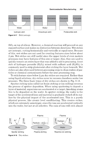
Photoresist Photoresist Photoresist Photoresist Photoresist Photoresist
Wafer Wafer Wafer
Isotropic etch Anisotropic etch Preferential etch
Figure 9-17 Etch isotropy.
SiO on top of silicon. However, a chemical reaction will proceed on any
2
exposed surface and makes no distinction between directions. Wet etches
are isotropic, cutting horizontally and vertically at equal rates. Because
of this, wet etches are not used for creating features sizes below about
2 µm. Wet etches are still useful since the upper levels of even modern
processes may have features of this size or larger. Also, they are used to
quickly remove an entire layer that was added to aid in processing. A wet
etch of hydrogen peroxide (H O ) mixed with sulfuric acid (H SO ) is
2
2
4
2
commonly used to strip photoresist after etching the layer beneath. Wet
etches are also often used between processing steps to clean wafers of par-
ticles or chemical contaminants before the next processing step.
To etch feature sizes below 2 µm dry etches are required. Rather than
using liquid solutions, dry etches occur in vacuum chambers under low
pressure. The three basic types of dry etches are shown in Fig. 9-18.
Sputter etching (also called ion beam etching or ion milling) reverses
the process of sputter deposition. When using sputtering to deposit a
layer of material, argon ions are accelerated at a target, knocking atoms
free to be deposited on the wafer. In sputter etching, the wafer is the
target of the accelerated ions and material is gradually etched off its sur-
face by the physical impact of the accelerated ions. This is a purely
physical process, like atomic level sandblasting. This creates etches,
which are extremely anisotropic, since the ions are accelerated vertically
into the wafer, but not at all selective. The rain of ions will etch almost
Plasma Plasma
E-field Ar + E-field Radical+ E-field Radical+ E-field
Wafer Wafer Wafer
Sputter etching Plasma etching Reactive ion etching
Figure 9-18 Dry etches.