
Page 321 - A Practical Guide from Design Planning to Manufacturing
P. 321
Semiconductor Manufacturing 291
B
A
B
A
SiO 2
B
N-well
Arsenic
PR
SiO 2 SiO 2
N-well A N-well A
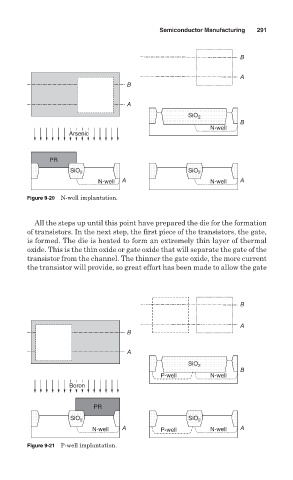
Figure 9-20 N-well implantation.
All the steps up until this point have prepared the die for the formation
of transistors. In the next step, the first piece of the transistors, the gate,
is formed. The die is heated to form an extremely thin layer of thermal
oxide. This is the thin oxide or gate oxide that will separate the gate of the
transistor from the channel. The thinner the gate oxide, the more current
the transistor will provide, so great effort has been made to allow the gate
B
A
B
A
SiO 2
B
P-well N-well
Boron
PR
SiO 2 SiO 2
N-well A P-well N-well A
Figure 9-21 P-well implantation.