
Page 325 - A Practical Guide from Design Planning to Manufacturing
P. 325
Semiconductor Manufacturing 295
B
A
B
A
Poly
O
O
O
O
O
iO
S S S S Si S S S S Si S S S S Si iO 2 2 2 2 2 2 2 2 2
O
iO
O
O
O
O
O
O
O
O
O
O
O
S S SiiO 2
P+ N+
P-well N-well
Boron
PR
O
O
O
O
O
iO
S S S S Si S S S S Si
iO
O
O
O
O
O
O
O
O
O
O
O
O
O
O
O
O
O
O
O
O
O
O
O
O
O
O
O
O
S S S S SiiOO
S S S S Si S S S S Si iO S S S S SiiO
O
O
iO
N+ N+ 2 2 2 2 2 2 2 2 2 2 P P N+ N+ 2 2 2 2 2 2 2 2 2 2 P+ P+
P-well N-well P-well N-well
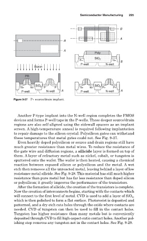
Figure 9-27 P+ source/drain implant.
Another P-type implant into the N-well region completes the PMOS
devices and forms P-well taps in the P-wells. These deeper source/drain
regions are also self-aligned using the sidewall spacers as an implant
screen. A high-temperature anneal is required following implantation
to repair damage to the silicon crystal. Polysilicon gates can withstand
these temperatures that metal gates could not. See Fig. 9-27.
Even heavily doped polysilicon or source and drain regions still have
much greater resistance than metal wires. To reduce the resistance of
the gate wire and diffusion regions, a silicide layer is formed on top of
them. A layer of refractory metal such as nickel, cobalt, or tungsten is
sputtered onto the wafer. The wafer is then heated, causing a chemical
reaction between exposed silicon or polysilicon and the metal. A wet
etch then removes all the unreacted metal, leaving behind a layer of low
resistance metal silicide. See Fig. 9-28. This material has still much higher
resistance than pure metal but has far less resistance than doped silicon
or polysilicon; it greatly improves the performance of the transistors.
After the formation of silicide, the creation of the transistors is complete.
Now the creation of interconnects begins, starting with the contacts which
,
will connect to the first level of metal. CVD is used to add a layer of SiO 2
which is then polished to form a flat surface. Photoresist is deposited and
patterned, and a dry etch cuts holes through the oxide where contacts are
needed. CVD of tungsten can then be used to fill in the contact holes.
Tungsten has higher resistance than many metals but is conveniently
deposited through CVD to fill high-aspect-ratio contact holes. Another pol-
ishing step removes any tungsten not in the contact holes. See Fig. 9-29.