
Page 323 - A Practical Guide from Design Planning to Manufacturing
P. 323
Semiconductor Manufacturing 293
B
B A
A
Poly
O
O
O
O
O
O
O
O
O
iO
iO
S S S S Si S S S S Si S S S S Si iO 2 2 2 2 2 2 2 2 2 2
S S SiiO
O
O
O
O
O
O
O
O
A Arsenic
P-well N-well
PR
O
S S S S Si S S S S Si
O
O
O
O
O
O
O
iO
O
O
O
O
O
O
O
iO
O
O
O
O
O
O
O
O
O
O
O
O
O
O
iO
O
iO
S S S S SiiOO S S S S SiiO
S S S S Si S S S S Si
O
O
O
O
O
2 2 2 2 2 2 2 2 2 2
N N 2 2 2 2 2 2 2 2 2 2
P-well N-well P-well N-well
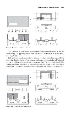
Figure 9-23 N-source/drain extension.
The creation of source and drain extensions is then repeated in the N-
wells using a P-type implant to form extensions for the PMOS transistors.
See Fig. 9-24.
Sidewalls are spacing structures created on either side of the gate, which
allow further implants of the source and drain regions to be self-aligned
to just outside the source/drain extensions. See Fig. 9-25. Silicon nitride
is deposited in a layer that is created to trace the shape of the structures
beneath it. This layer is the thickest on the vertical sides of the poly lines.
B
B A
A
Poly
O
O
O
O
O
O
O
O
S S SiiO 2 2 2 2 2 2 2 2 2 2
S S S S Si S S S S Si S S S S Si
O
iO
iO
iO
O
O
O
O
O
O
O
O
Boron n P-well N-well
PR
O
O
O
O
O
O
O
O
O
O
O
O
O
O
O
O
O
O
O
O
O
O
O
O
O
O
O
S S S S SiiO
iO
O
O
S S S S SiiO
O
S S S S Si S S S S Si iO S S S S Si S S S S Si iO
O
O
O
O
O
O
iO
N N 2 2 2 2 2 2 2 2 2 2 N N 2 2 2 2 2 2 2 2 2 2 P P
P-well N-well P-well N-well
Figure 9-24 P-source/drain extension.