
Page 327 - A Practical Guide from Design Planning to Manufacturing
P. 327
Semiconductor Manufacturing 297
style of ancient Damascus) on metal or ceramics made by pouring metal
into grooves carved in the surface. In semiconductor manufacturing, dam-
ascene processes contain copper by depositing the metal into grooves of
insulation.
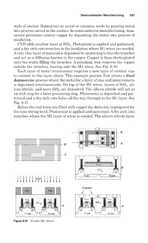
CVD adds another layer of SiO 2 . Photoresist is applied and patterned,
and a dry etch cuts trenches in the insulation where M1 wires are needed.
Avery thin layer of material is deposited by sputtering to line the trenches
and act as a diffusion barrier to the copper. Copper is then electroplated
onto the wafer filling the trenches. A polishing step removes the copper
outside the trenches, leaving only the M1 wires. See Fig. 9-30.
Each layer of metal interconnect requires a new layer of vertical vias
to connect to the layer above. This example process flow shows a dual
damascene process where the metal for a layer of vias and interconnects
is deposited simultaneously. On top of the M1 wires, layers of SiO , sil-
2
icon nitride, and more SiO are deposited. The silicon nitride will act as
2
an etch stop for a later processing step. Photoresist is deposited and pat-
terned and a dry etch cuts holes all the way through to the M1 layer. See
Fig. 9-31.
Before the vial holes are filled with copper the dielectric is prepared for
the next wiring level. Photoresist is applied and patterned. Adry etch cuts
trenches where the M2 layer of wires is needed. The silicon nitride layer
B
B A
A
M1
Poly
B
O
O
O
O
O
S S S S Si S S S S Si
S S S S SiO
O
O
O
O
O
O
O
O
O
O
O
O
P+ 2 2 2 2 2 2 2 2 2 2 2 N+
P-well N-well
Etch
Copper
PR PR
M1
P P P Po
P P P P P P P P
o
P Poooly
o
oly
o
o
o
ol
ol
oly
o
o
l
l
l
P P P
P P P Po
P P Pooly y y y y y y y y y P P P P P P Po o o ol o l l l y y y y y y y P P P Po o oly l l y y y y y y y y P Pooly y y y y y y y y y
o
o
P P Poooly
O
O
O
O
O
O
O
O
O
O
O
S S S S Si S S S S Si S S Si
O
O
O
O
O
O
O
O
O
O
O
O
O
O
O
O
O
O
O
O
S S S S SiiO 2 2 2 2 2 2 2 2 2 2 2 2 S S SiO 2 2 2 2 2 2 2 2 2 2 2
O
S S S S Si S S S S Si
iO
iO
A A
N+ N+ P+ P+ N+ N+ P+ P+
P-well N-well P-well N-well
Figure 9-30 Create M1 wires.