
Page 322 - A Practical Guide from Design Planning to Manufacturing
P. 322
292 Chapter Nine
B
B
A
A
Poly
Etch SiO 2
B
P-well N-well
PR
Poly Poly
Poly
SiO 2 A SiO
P-well N-well 2
P-well N-well A
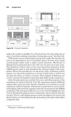
Figure 9-22 Poly gate formation.
oxide to be as thin as possible. In a 90-nm process, the gate oxide may be
4
only 1.2 nm thick, making it less than 10 molecules across. See Fig. 9-22.
CVD creates a layer of polysilicon on top of the oxide. Because the sil-
icon is not deposited on top of crystalline silicon, it forms many small
crystal grains rather than a single crystal structure. Photoresist is
deposited and patterned and a dry etch cuts the poly layer into wires.
The thickness of these wires is the most important dimension of the
CMOS process since it will determine the channel length of the tran-
sistors. Where the polysilicon is on top of gate oxide, transistors will be
formed, but where the polysilicon is on top of field oxide, it will be too
far from the silicon to create a channel. These lengths of field poly are
used to connect the lengths of gate poly that make up the transistors.
After the poly gates are created, the source and drain regions of the
transistors are formed. See Fig. 9-23. The extensions of these diffusion
regions that reach up to the channel should be very shallow to create
transistors with low leakage. Photoresist is patterned to screen the N-
well regions, and an N-type implant forms the extensions for the NMOS
transistors. The poly gate itself acts as a screen for the implant into the
P-well, blocking the dopants from reaching the silicon directly beneath
the poly. This is a self-aligned process where the edges of the source and
drain regions are determined by the patterning of the poly rather than
a separate step.
4
Thompson, “A 90nm Logic Technology.”