
Page 320 - A Practical Guide from Design Planning to Manufacturing
P. 320
290 Chapter Nine
B
A
B
A
SiO 2
B
Silicon wafer
Etch
N
PR Si 3 4 PR
SiO
A 2
Silicon wafer A
Silicon wafer
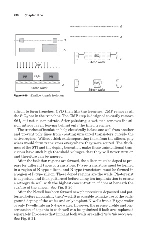
Figure 9-19 Shallow trench isolation.
silicon to form trenches. CVD then fills the trenches. CMP removes all
the SiO not in the trenches. The CMP step is designed to easily remove
2
SiO but not silicon nitride. After polishing, a wet etch removes the sil-
2
icon nitride layer, leaving behind only the filled trenches.
The trenches of insulation help electrically isolate one well from another
and prevent poly lines from creating unwanted transistors outside the
active regions. Without thick oxide separating them from the silicon, poly
wires would form transistors everywhere they were routed. The thick-
ness of the STI and the doping beneath it make these unintentional tran-
sistors have such high threshold voltages that they will never turn on
and therefore can be ignored.
After the isolation regions are formed, the silicon must be doped to pre-
pare for different types of transistors. P-type transistors must be formed
in a region of N-type silicon, and N-type transistors must be formed in
a region of P-type silicon. These doped regions are the wells. Photoresist
is deposited and then patterned before using ion implantation to create
a retrograde well with the highest concentration of dopant beneath the
surface of the silicon. See Fig. 9-20.
After the N-well has been formed new photoresist is deposited and pat-
terned before implanting the P-well. It is possible to make use of the back-
ground doping of the wafer and only implant N-wells into a P-type wafer
or only P-wells into an N-type wafer. However, the precise profile and con-
centration of dopants in each well can be optimized if both are implanted
separately. Processes that implant both wells are called twin tub processes.
See Fig. 9-21.