
Page 324 - A Practical Guide from Design Planning to Manufacturing
P. 324
294 Chapter Nine
B
A
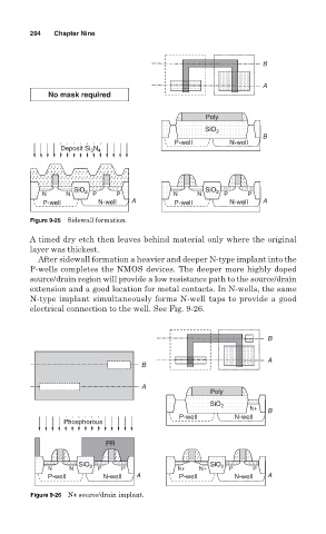
No mask required
Poly
O
O
O
O
iO
S S S S Si S S S S Si S S S S Si iO 2 2 2 2 2 2 2 2 2
iO
O
O
O
O
O
O
O
O
O
O
O
O
O
S S SiiO 2
P-well N-well
Deposit Si N
3 4
O
O
O
O
O
O
O
O
O
O
S S S S SiiO S S S S Si S S S S Si iO
O
S S S S SiiO
iO
iO
O
O
S S S S Si S S S S Si
iO
O
O
O
O
O
O
O
O
O
O
O
O
O
O
O
O
O
O
O
O
O
O
O
N N 2 2 2 2 2 2 2 2 2 2 P P N N 2 2 2 2 2 2 2 2 2 2 P P
P-well N-well P-well N-well
Figure 9-25 Sidewall formation.
A timed dry etch then leaves behind material only where the original
layer was thickest.
After sidewall formation a heavier and deeper N-type implant into the
P-wells completes the NMOS devices. The deeper more highly doped
source/drain region will provide a low resistance path to the source/drain
extension and a good location for metal contacts. In N-wells, the same
N-type implant simultaneously forms N-well taps to provide a good
electrical connection to the well. See Fig. 9-26.
B
A
B
A
Poly
O
O
O
O
O
iO
iO
O
O
O
O
O
O
O
O
O
O
O
O
S S S S Si S S S S Si S S S S Si iO
S S SiiO
2 2 2 2 2 2 2 2 2 2
N+
P-well N-well
Phosphorous
PR
O
O
O
O
O
O
O
O
O
O
O
O
O
iO
O
O
O
O
O
O
O
O
O
O
O
O
O
O
O
iO
iO
O
O
S S S S SiiOO S S S S SiiO
O
O
iO
O
O
O
S S S S Si S S S S Si
S S S S Si S S S S Si
N N 2 2 2 2 2 2 2 2 2 2 P P N+ N+ 2 2 2 2 2 2 2 2 2 2 P P
P-well N-well P-well N-well
Figure 9-26 N+ source/drain implant.