
Page 328 - A Practical Guide from Design Planning to Manufacturing
P. 328
298 Chapter Nine
B
A
B
A
Si N 4 4
3 3 3 3 4
M1
B
Etch Poly
O
O
O
O
O
S S SiO
S S S S Si S S S S Si S S Si
O
O
O
O
O
O
O
O
O
O
O
O
P+ 2 2 2 2 2 2 2 2 2 2 2 N+
P-well N-well
PR PR
Si N 4 4 Si N 4 4 4
3 3 3 4
3 3 3 4
M1 M1
o
o
ol
o
P P P Po
o
o
o
o
o
P P P P P
P P Pooly
o
P P P P P
P P P Po
o
oly
o
o
oly
o
P P Poooly l l l l y y y y y y y y y P P P P P P P Pooly l l l l y y y y y y y P P Poooly l l l l y y y y y y y y y P P P Po o ol l l l l y y y y y y y
P P P Po
P P P P P
O
O
O
O
iO
O
O
O
O
O
O
O
O
O
O
O
O
O
O
O
O
O
O
O
O
O
O
S S S S Si S S S S Si
iO
S S S S Si S S S S Si
iO
S S S S SiiO 2 2 2 2 2 2 2 2 2 2 2 S S S S SiiO 2 2 2 2 2 2 2 2 2 2 2
iO
O
O
O
O
A A
N+ N+ P+ P+ N+ N+ P+ P+
P-well N-well P-well N-well
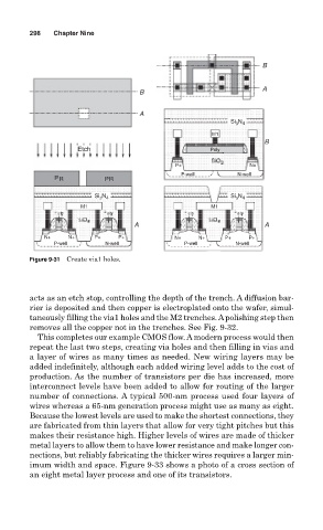
Figure 9-31 Create via1 holes.
acts as an etch stop, controlling the depth of the trench. A diffusion bar-
rier is deposited and then copper is electroplated onto the wafer, simul-
taneously filling the via1 holes and the M2 trenches. Apolishing step then
removes all the copper not in the trenches. See Fig. 9-32.
This completes our example CMOS flow. A modern process would then
repeat the last two steps, creating via holes and then filling in vias and
a layer of wires as many times as needed. New wiring layers may be
added indefinitely, although each added wiring level adds to the cost of
production. As the number of transistors per die has increased, more
interconnect levels have been added to allow for routing of the larger
number of connections. A typical 500-nm process used four layers of
wires whereas a 65-nm generation process might use as many as eight.
Because the lowest levels are used to make the shortest connections, they
are fabricated from thin layers that allow for very tight pitches but this
makes their resistance high. Higher levels of wires are made of thicker
metal layers to allow them to have lower resistance and make longer con-
nections, but reliably fabricating the thicker wires requires a larger min-
imum width and space. Figure 9-33 shows a photo of a cross section of
an eight metal layer process and one of its transistors.