
Page 330 - A Practical Guide from Design Planning to Manufacturing
P. 330
300 Chapter Nine
Conclusion
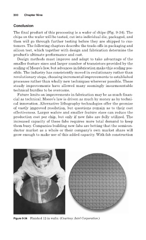
The final product of this processing is a wafer of chips (Fig. 9-34). The
chips on the wafer will be tested, cut into individual die, packaged, and
then will go through further testing before they are shipped to cus-
tomers. The following chapters describe the trade-offs in packaging and
silicon test, which together with design and fabrication determine the
product’s ultimate performance and cost.
Design methods must improve and adapt to take advantage of the
smaller feature sizes and larger number of transistors provided by the
scaling of Moore’s law, but advances in fabrication make this scaling pos-
sible. The industry has consistently moved in evolutionary rather than
revolutionary steps, choosing incremental improvements to established
processes rather than wholly new techniques wherever possible. These
steady improvements have allowed many seemingly insurmountable
technical hurdles to be overcome.
Future limits on improvements in fabrication may be as much finan-
cial as technical. Moore’s law is driven as much by money as by techni-
cal innovation. Alternative lithography technologies offer the promise
of vastly improved resolution, but questions remain as to their cost
effectiveness. Larger wafers and smaller feature sizes can reduce the
production cost per chip, but only if new fabs are fully utilized. The
increased capacity of these fabs requires more total demand to keep
them busy. Companies building new fabs are betting that the semicon-
ductor market as a whole or their company’s own market share will
grow enough to make use of this added capacity. With fab construction
Figure 9-34 Finished 12-in wafer. (Courtesy: Intel Corporation.)