
Page 345 - A Practical Guide from Design Planning to Manufacturing
P. 345
Microprocessor Packaging 315
Step #1 Step #2
Blanking Via punch and fill
Step #3 Step #4
Conductor print Laminate and cofire
Apply heat and pressure
Step #5 Step #6
Pin braze Die attach and wire bond
Die
Die cavity
Pin
Lid
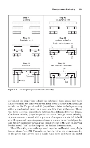
Figure 10-6 Ceramic package formation and assembly.
sections of the proper size to form the substrate. Some pieces may have
a hole cut from the center that will later form a cavity in the package
to hold the die. Via punch and fill (step #2) cuts holes in the layers using
either a mechanical punch or a laser and fills them with metal. These
will form electrical connections between the different layers of traces.
Conductor printing (step #3) applies the traces through screen printing.
A porous screen covered with a pattern of nonporous material is held
over the pieces of tape. A squeegee forces a viscous mix of metal powder
and binder chemicals through the open portions of the screen, leaving
behind metal “ink” in the shape of the desired interconnects.
The different layers are then pressed together and heated to very high
temperatures (step #4). This cofiring fuses together the ceramic powder
of the green tape layers into a single rigid piece and fuses the metal