
Page 348 - A Practical Guide from Design Planning to Manufacturing
P. 348
318 Chapter Ten
package shown in Fig. 10-7 could be described as a six-layer package
because of the six separate layers of interconnect. More specifically, it
might be called a 1-4-1 layer package because the package has 1 buildup
layer on top, 4 core interconnect layers in the center, and 1 buildup layer
on the bottom. The number of layers needed is dictated by the total lead
count of the package as well as the package size. More layers allow for
denser interconnect and a smaller package but increase the cost of pack-
aging. Once again there is no perfect package.
Die attach
Die attach refers to how the die will be physically and electrical connected
to the package substrate. The previous section has described the die
attach method of wire bond. Wire bond is the most commonly used and
the cheapest method of die attach, but it has a number of disadvantages.
In wire bond, the placement of the bonding pads on the die and on the
substrate must be carefully chosen to avoid wires to different pads touch-
ing. Multiple tiers of bonding pads in the substrate can help, but the die
bonding pads are still restricted to only the perimeter of the chip. For die
with a large number of leads but a small number of transistors, this can
lead to the die size being limited not by the transistors needed but by the
number of bonding pads required. For these reasons, wire bond is typi-
cally not used with die requiring more than a few hundred leads. The
length of the wires used to connect die to substrate is also a concern.
These wires will add capacitance and inductance to the leads and limit
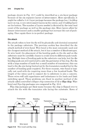
switching speed. These problems are fixed in another method of die
attach called controlled collapse chip connection (C4) or flip-chip. Wire
bond and flip-chip packages are compared in Fig. 10-8.
Flip-chip packages get their name because the chip is flipped over to
attach the die with the transistor side facing the substrate. Rows of
Transistors Bonding C4 Bump
pad Transistors Underfill
Die
Die
Wire bond Flip-chip
Figure 10-8 Wire bond and flip-chip.