
Page 347 - A Practical Guide from Design Planning to Manufacturing
P. 347
Microprocessor Packaging 317
Step #1 Step #2
Core layers Drill and pattern layers
Copper foil Via Trace
FR4
Step #3 Step #4
Interleave prepreg, laminate and drill Apply buildup layers
Solder mask
Apply heat and pressure
Prepreg
Buildup layer
Step #5 Step #6
Pin braze Die attach and wire bond
Lid Die
Pin
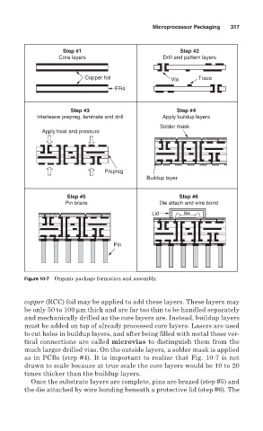
Figure 10-7 Organic package formation and assembly.
copper (RCC) foil may be applied to add these layers. These layers may
be only 50 to 100 µm thick and are far too thin to be handled separately
and mechanically drilled as the core layers are. Instead, buildup layers
must be added on top of already processed core layers. Lasers are used
to cut holes in buildup layers, and after being filled with metal these ver-
tical connections are called microvias to distinguish them from the
much larger drilled vias. On the outside layers, a solder mask is applied
as in PCBs (step #4). It is important to realize that Fig. 10-7 is not
drawn to scale because at true scale the core layers would be 10 to 20
times thicker than the buildup layers.
Once the substrate layers are complete, pins are brazed (step #5) and
the die attached by wire bonding beneath a protective lid (step #6). The