
Page 365 - A Practical Guide from Design Planning to Manufacturing
P. 365
Silicon Debug and Test 335
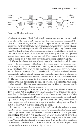
Scan F-F F-F Scan
input output
F-F F-F
Input Cycle 1 F-F Cycle 2 F-F Cycle 3 Output
pins logic logic logic pins
F-F F-F
Figure 11-3 Nondestructive scan.
of values that are serially shifted into all the scan sequentials. Asingle clock
cycle allows the values to be driven into the combinational logic, and the
results are then serially shifted to an output pin to be checked. Both observ-
ability and controllability are vastly improved. Amismatch in captured scan
values from what is expected will tell exactly which pipestage has the prob-
lem. One disadvantage of this implementation of scan is that it is destruc-
tive. This means that as scan values are serially shifted through the
sequentials, the original values are lost. This makes it difficult to restart
the processor after it has been stopped and the scan values read out.
Different implementations of scan may add complexity and die area
in order to allow improved testing or have less impact on normal oper-
ation. Figure 11-3 shows the scan chain implemented as a separate set
of sequentials. The circuits are designed so a special capture signal
causes the scan sequentials to store the value of their associated normal
sequentials. A load signal causes the normal sequentials to change to
the value of the scan sequentials. This mechanism and a separate clock
for the scan chain allows for the scan chain to capture and read out
values without disturbing normal operation, a nondestructive scan
implementation. Nondestructive scan enables rapid capture of many dif-
ferent points in time during a single test.
The best coverage is provided by making every sequential scannable.
This is called full scan. However, the area penalty for this may be exces-
sive. Many designs choose partial scan where some fraction of the
sequentials are scannable. Faults may have to propagate through mul-
tiple cycles of logic before reaching a scannable element, which makes
tests longer to get the same coverage and makes debug more difficult,
but it is still vastly simpler than with no scan.
To keep test time to a minimum, it is useful to calculate the minimum
number of test vectors needed to check for possible faults. Using CAD
tools to generate these test vectors is called automatic test pattern
generation (ATPG). ATPG must assume a fault model, which describes
how a design flaw or manufacturing defect may appear in functional
tests. The simplest and most commonly used fault model is the stuck-at
fault model. This assumes that defects can make any node appear to be
permanently stuck at a low or a high voltage.