
Page 363 - A Practical Guide from Design Planning to Manufacturing
P. 363
Silicon Debug and Test 333
This is the process of silicon test. Only an extremely small fraction of die
will ever go through the added steps of silicon debug to try and charac-
terize design flaws. Every die manufactured must go through silicon
test before being shipped. It is critical that this process is quick to keep
costs down and is thorough to avoid shipping defective die.
To aid in post-silicon validation, silicon debug, and silicon test, all
modern processors add some circuits used specifically for testing. These
are called design for test (DFT) circuits.
Design for Test Circuits
DFT circuits are special in that the customer never uses them. Every
processor die uses some amount of area and some amount of power for cir-
cuits that are never used during the normal operation of the chip. However,
without these circuits, validation and test would be almost impossible.
The problem is the decreasing observability and controllability of
processors. Without DFT circuits, the only signals that can be directly
observed or controlled are the processor pins. The number of processor
pins is increasing but far more slowly than the number of total tran-
sistors. This makes it more difficult with each processor generation to
directly read or write a specific node within the design by the use of the
pins alone. DFT circuits help by expanding observability and control-
lability. DFT increases the cost of the design by taking up die area and
consuming some leakage power. DFT circuits also impact processor fre-
quency, and their complexity can increase the design time to tapeout.
However, the benefits of DFT circuits during post-silicon validation are
so great that all modern designs use at least some DFT circuits. By
aiding silicon debug, DFT reduces the number of design steppings
required to fix bugs. This reduces the time from tapeout to shipping and
saves costs by reducing the number of mask sets created. Also, shipping
costs are reduced by shorter test time, allowing for less test equipment
and fewer defects shipped.
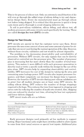
DFT circuit trade-offs are as follows:
Disadvantages Advantages
Increased design time to tapeout Reduced time from tapeout to shipping
Added die area Fewer post-silicon design revisions
Added leakage power Shorter test time to identify defects
May reduce frequency Fewer defects shipped
Early processor designs used primarily ad hoc methods to support
testing. Major functional units might have switches added to allow inputs
to come from their usual sources or special test inputs. Additional pins