
Page 364 - A Practical Guide from Design Planning to Manufacturing
P. 364
334 Chapter Eleven
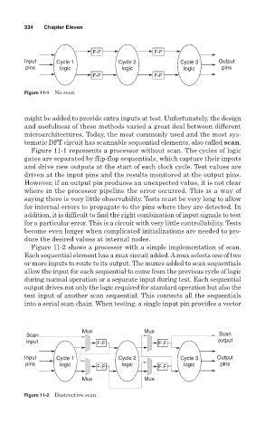
F-F F-F
Input Cycle 1 Cycle 2 Cycle 3 Output
pins logic logic logic pins
F-F F-F
Figure 11-1 No scan.
might be added to provide extra inputs at test. Unfortunately, the design
and usefulness of these methods varied a great deal between different
microarchitectures. Today, the most commonly used and the most sys-
tematic DFT circuit has scannable sequential elements, also called scan.
Figure 11-1 represents a processor without scan. The cycles of logic
gates are separated by flip-flop sequentials, which capture their inputs
and drive new outputs at the start of each clock cycle. Test values are
driven at the input pins and the results monitored at the output pins.
However, if an output pin produces an unexpected value, it is not clear
where in the processor pipeline the error occurred. This is a way of
saying there is very little observability. Tests must be very long to allow
for internal errors to propagate to the pins where they are detected. In
addition, it is difficult to find the right combination of input signals to test
for a particular error. This is a circuit with very little controllability. Tests
become even longer when complicated initializations are needed to pro-
duce the desired values at internal nodes.
Figure 11-2 shows a processor with a simple implementation of scan.
Each sequential element has a mux circuit added. Amux selects one of two
or more inputs to route to its output. The muxes added to scan sequentials
allow the input for each sequential to come from the previous cycle of logic
during normal operation or a separate input during test. Each sequential
output drives not only the logic required for standard operation but also the
test input of another scan sequential. This connects all the sequentials
into a serial scan chain. When testing, a single input pin provides a vector
Mux Mux
Scan Scan
input F-F F-F output
Input Cycle 1 Cycle 2 Cycle 3 Output
pins logic F-F logic F-F logic pins
Mux Mux
Figure 11-2 Destructive scan.