Page 366 - A Practical Guide from Design Planning to Manufacturing
P. 366
336   Chapter Eleven


               A        Y
               B                Z
               C
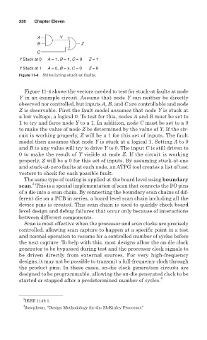
        Y Stuck at 0  A = 1, B = 1, C = 0  Z = 1
        Y Stuck at 1  A = 0, B = x, C = 0  Z = 0
        Figure 11-4 Stimulating stuck-at faults.

          Figure 11-4 shows the vectors needed to test for stuck-at faults at node
        Y in an example circuit. Assume that node Y can neither be directly
        observed nor controlled, but inputs A, B, and C are controllable and node
        Z is observable. First the fault model assumes that node Y is stuck at
        a low voltage, a logical 0. To test for this, nodes A and B must be set to
        1 to try and force node Y to a 1. In addition, node C must be set to a 0
        to make the value of node Z be determined by the value of Y. If the cir-
        cuit is working properly, Z will be a 1 for this set of inputs. The fault
        model then assumes that node Y is stuck at a logical 1. Setting A to 0
        and B to any value will try to drive Y to 0. The input C is still driven to
        0 to make the result of Y visible at node Z. If the circuit is working
        properly, Z will be a 0 for this set of inputs. By assuming stuck-at-one
        and stuck-at-zero faults at each node, an ATPG tool creates a list of test
        vectors to check for each possible fault.
          The same type of testing is applied at the board level using boundary
             3
        scan. This is a special implementation of scan that connects the I/O pins
        of a die into a scan chain. By connecting the boundary scan chains of dif-
        ferent die on a PCB in series, a board level scan chain including all the
        device pins is created. This scan chain is used to quickly check board
        level design and debug failures that occur only because of interactions
        between different components.
          Scan is most effective when the processor and scan clocks are precisely
        controlled, allowing scan capture to happen at a specific point in a test
        and normal operation to resume for a controlled number of cycles before
        the next capture. To help with this, most designs allow the on-die clock
        generator to be bypassed during test and the processor clock signals to
        be driven directly from external sources. For very high-frequency
        designs, it may not be possible to transmit a full-frequency clock through
        the product pins. In these cases, on-die clock generation circuits are
        designed to be programmable, allowing the on-die generated clock to be
        started or stopped after a predetermined number of cycles. 4


          3
          IEEE 1149.1.
          4
          Josephson, “Design Methodology for the McKinley Processor.”

