
Page 358 - A Practical Guide from Design Planning to Manufacturing
P. 358
328 Chapter Ten
Step #1 Step #2
Substrate formation Die attach
Decap
Via
Die
Pin
Step #3 Step #4
Underfill Lid attach
IHS
Underfill
Die Die
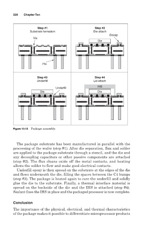
Figure 10-13 Package assembly.
The package substrate has been manufactured in parallel with the
processing of the wafer (step #1). After die separation, flux and solder
are applied to the package substrate through a stencil, and the die and
any decoupling capacitors or other passive components are attached
(step #2). The flux cleans oxide off the metal contacts, and heating
allows the solder to flow and make good electrical contacts.
Underfill epoxy is then spread on the substrate at the edges of the die
and flows underneath the die, filling the spaces between the C4 bumps
(step #3). The package is heated again to cure the underfill and solidly
glue the die to the substrate. Finally, a thermal interface material is
spread on the backside of the die and the IHS is attached (step #4).
Sealant fixes the IHS in place and the packaged processor is now complete.
Conclusion
The importance of the physical, electrical, and thermal characteristics
of the package makes it possible to differentiate microprocessor products