
Page 356 - A Practical Guide from Design Planning to Manufacturing
P. 356
326 Chapter Ten
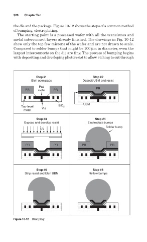
the die and the package. Figure 10-12 shows the steps of a common method
of bumping, electroplating.
The starting point is a processed wafer with all the transistors and
metal interconnect layers already finished. The drawings in Fig. 10-12
show only the top few microns of the wafer and are not drawn to scale.
Compared to solder bumps that might be 100 µm in diameter, even the
largest interconnects on the die are tiny. The process of bumping begins
with depositing and developing photoresist to allow etching to cut through
Step #1 Step #2
Etch open pads Deposit UBM and resist
Pad
PR metal PR PR
UBM
Top-level Via SiO 2
metal
Step #3 Step #4
Expose and develop resist Electroplate bumps
Solder bump
UV
PR PR PR PR
Step #5 Step #6
Strip resist and Etch UBM Reflow bumps
Figure 10-12 Bumping.