
Page 168 - Microsensors, MEMS and Smart Devices - Gardner Varadhan and Awadelkarim
P. 168
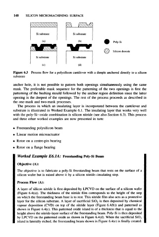
148    SILICON  MICROMACHINING: SURFACE
                                   m      mrm


                   Si substrate        Si  substrate

                      (a)                 (b)                 Poly-Si

                                                             Silicon dioxide
                   Si  substrate       Si  substrate

                      (c)                 (d)
      Figure 6.3  Process flow for a polysilicon  cantilever  with a dimple  anchored  directly  to a  silicon
      substrate
      anchor  hole,  it  is  not  possible  to  pattern  both  openings  simultaneously  using  the  same
      mask.  The  preferable  mask  sequence  for  the  patterning of  the  two  openings  is  first  the
      patterning  of  the  bushing  mould followed  by  the  anchor  region  definition  since  the  latter
      opening  is  the  deepest  of  the  openings.  The  rest  of  the  process  proceeds  as  described  in
      the  one-mask  and two-mask  processes.
        The  process  in  which  an  insulating layer  is  incorporated  between  the  cantilever  and
      substrate  is illustrated in Worked Example  6.1.  The  insulating  layer that works very  well
      with the poly-Si-oxide combination  is silicon  nitride  (see  also  Section  6.3).  This  process
      and  three  other  worked  examples  are  now presented  in turn:


      •  Freestanding  polysilicon  beam
      •  Linear  motion microactuator
      •  Rotor on a centre-pin bearing
      •  Rotor  on a flange  bearing

        Worked  Example   E6.1A:  Freestanding  Poly-Si  Beam

        Objective  (A):
        The  objective  is to fabricate  a poly-Si  freestanding  beam that  rests on  the  surface  of a
        silicon  wafer  but  is raised  above it by a silicon nitride-insulating step.

        Process Flow  (A):
        A layer of  silicon  nitride is first deposited by  LPCVD on the  surface  of a silicon  wafer
        (Figure 6.4(a)).  The  thickness  of  the  nitride  film  corresponds  to  the  height  of  the  step
        on which  the freestanding  beam base is to rest. This  nitride film also acts as a protective
        layer for the  silicon  substrate.  A layer of  sacrificial  SiO 2  is then  deposited by  chemical
        vapour  deposition  (CVD)  on  top  of  the  nitride  layer  (Figure 6.4(b))  and  patterned  as
        shown  in Figure 6.4(c). This patterned oxide island is of a thickness that  is equal to the
        height above the nitride-layer surface  of the freestanding  beam. Poly-Si is then deposited
        by LPCVD on the patterned oxide as shown  in Figure 6.4(d). When  the  sacrificial  SiO 2
        island  is laterally  etched, the freestanding  beam  shown  in Figure  6.4(e) is finally created.