
Page 169 - Microsensors, MEMS and Smart Devices - Gardner Varadhan and Awadelkarim
P. 169
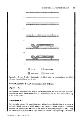
SACRIFICIAL  LAYER  TECHNOLOGY    149


                        (a)


                        (b)


                        (c)


                               Poly-Si        Silicon dioxide

                               Silicon nitride  (Silicon) substrate
        Figure 6.4  Process flow for a freestanding  polysilicon  cantilever beam anchored  to a  silicon
        substrate  via  an insulating  nitride  layer


        Worked  Example  E6.1B:  Freestanding  Poly-Si  Beam 3
        Objective  (B):

        The  objective  is  to fabricate  a poly-Si  freestanding  beam  that rests  on  the  surface of a
        silicon  wafer and  is  on the  same  level  as  a nitride layer  that has  been  deposited  on  top
        of  the  silicon wafer.


        Process Flow  (B):
        This  second procedure  for  beam fabrication is  based  on  the localised oxide isolation of
        silicon  (LOCOS)  process in which windows are  opened  in  silicon  nitride  on the silicon
        substrate and, subsequently, thermal SiO2 is grown in the openings  (Figure  6.5(a)).  Using
        this patterned  SiO 2 as a sacrificial  layer allows the construction of planar poly-Si  beams.


      For  details  see Linder et al.  (1992).