
Page 171 - Microsensors, MEMS and Smart Devices - Gardner Varadhan and Awadelkarim
P. 171
151
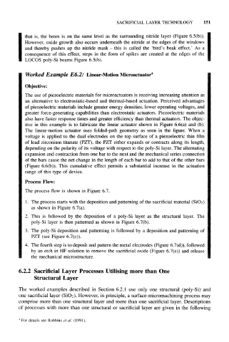
that is, the beam is on the same level as the surrounding nitride layer (Figure 6.5(b)).
However, oxide growth also occurs underneath the nitride at the edges of the windows
and thereby pushes up the nitride mask - this is called the 'bird's beak effect.' As a
consequence of this effect, steps in the form of spikes are created at the edges of the
LOCOS poly-Si beams Figure 6.5(b).
Worked Example E6.2: Linear-Motion Microactuator 4
Objective:
The use of piezoelectric materials for microactuators is receiving increasing attention as
an alternative to electrostatic-based and thermal-based actuation. Perceived advantages
of piezoelectric materials include greater energy densities, lower operating voltages, and
greater force-generating capabilities than electrostatic actuators. Piezoelectric materials
also have faster response times and greater efficiency than thermal actuators. The objec-
tive in this example is to fabricate the linear actuator shown in Figure 6.6(a) and (b).
The linear-motion actuator uses folded-path geometry as seen in the figure. When a
voltage is applied to the dual electrodes on the top surface of a piezoelectric thin film
of lead zirconium titanate (PZT), the PZT either expands or contracts along its length,
depending on the polarity of its voltage with respect to the poly-Si layer. The alternating
expansion and contraction from one bar to the next and the mechanical series connection
of the bars cause the net change in the length of each bar to add to that of the other bars
(Figure 6.6(b)). This cumulative effect permits a substantial increase in the actuation
range of this type of device.
Process Flow:
The process flow is shown in Figure 6.7.
1. The process starts with the deposition and patterning of the sacrificial material (SiO2)
as shown in Figure 6.7(a).
2. This is followed by the deposition of a poly-Si layer as the structural layer. The
poly-Si layer is then patterned as shown in Figure 6.7(b).
3. The poly-Si deposition and patterning is followed by a deposition and patterning of
PZT (see Figure 6.7(c)).
4. The fourth step is to deposit and pattern the metal electrodes (Figure 6.7(d)), followed
by an etch in HF solution to remove the sacrificial oxide (Figure 6.7(e)) and release
the mechanical microstructure.
6.2.2 Sacrificial Layer Processes Utilising more than One
Structural Layer
The worked examples described in Section 6.2.1 use only one structural (poly-Si) and
one sacrificial layer (SiO 2). However, in principle, a surface-micromachining process may
comprise more than one structural layer and more than one sacrificial layer. Descriptions
of processes with more than one structural or sacrificial layer are given in the following
4
For details see Robbins et al. (1991).