
Page 262 - Microsensors, MEMS and Smart Devices - Gardner Varadhan and Awadelkarim
P. 262
242 MICROSENSORS
Radiation
Photoconductive
material
Electrode
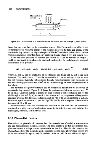
Figure 8.14 Basic layout of a photoconductive cell with a constant voltage V o drive circuit
holes that can contribute to the conduction process. This Photoconductive effect is the
dominant process when the energy of the radiation is above the band gap energy of the
semiconducting material. At higher energies, of 100 keV and above, other effects, such as
Compton scattering, occur but these only apply for detecting hard X rays and gamma rays.
If the radiation produces N t carriers per second in a slab of material of length /,
width w, and depth d, its change in electrical conductivity Aa and change in electrical
conductance G is given by
wd
Aa = + and so AG = r n + — (8.18)
where /n n and /x p are the mobilities of the electrons and holes and r n and r p are their
lifetimes. The conductance I/V o can be measured in a constant voltage V o circuit with
the cell resistance typically falling almost linearly with illuminance from megaohms in
the dark (band gap exceeds the 1/40 th eV of thermal energy at room temperature) to a
few ohms.
The response of a photoconductive cell to radiation is determined by the choice of
semiconducting material. Figure 8.15 shows the various materials used to cover the UV
to IR range. Cadmium sulfide is commonly used to make a photoconductive cell for the
visible region (0.4 to 0.7 u.m) because it is inexpensive and easy to process, although other
materials are used for IR photoconductors, such as PbS with a peak response at 2.2 um,
PbSe with a peak response at 2.2 u.m, and HgCdTe (MCT) with a response tailored within
the range of 12 to 16 um.
Photoconductive cells are commercially available at low cost and are commonly
employed in a wide range of applications; examples include light-activated switches for
night lights, dimmers, and children's toys.
8.3.2 Photovoltaic Devices
Photovoltaic, or photoelectric, sensors form the second class of radiation microsensors
and are potentiometric radiation sensors. The basic principle is that the radiation (i.e.
photons) induces a voltage across a semiconductor junction; this effect is known as the
photovoltaic effect. The materials most commonly used to make photovoltaic sensors are
Si for the visible/NIR region, and Ge, InGaAs, InAs, or InSb for the NIR-to-IR region.