
Page 368 - Microsensors, MEMS and Smart Devices - Gardner Varadhan and Awadelkarim
P. 368
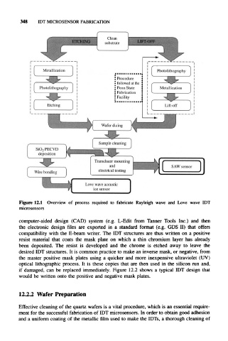
348    IDT MICROSENSOR  FABRICATION


  Figure  12.1  Overview  of  process  required  to  fabricate  Rayleigh  wave  and  Love  wave  IDT
  microsensors


  computer-aided  design  (CAD)  system  (e.g.  L-Edit  from  Tanner  Tools  Inc.)  and  then
  the  electronic  design  files  are  exported  in  a  standard  format  (e.g.  GDS  II)  that  offers
  compatibility  with the  E-beam  writer.  The  IDT structures are  thus written on  a  positive
  resist  material  that  coats  the  mask  plate  on  which  a  thin  chromium  layer  has  already
  been  deposited.  The  resist  is  developed  and  the  chrome  is  etched  away  to  leave  the
  desired IDT structures. It is common  practice  to make an inverse mask, or negative,  from
  the  master  positive  mask  plates  using a  quicker  and  more  inexpensive ultraviolet (UV)
  optical  lithographic  process.  It  is  these  copies  that are  then  used  in  the  silicon  run  and,
  if  damaged,  can  be  replaced  immediately.  Figure  12.2  shows  a  typical  IDT  design  that
  would  be written onto  the  positive  and negative  mask  plates.


  12.2.2  Wafer Preparation

  Effective  cleaning  of the quartz wafers is a vital procedure,  which is an essential  require-
  ment for the successful fabrication of IDT microsensors.  In order  to obtain  good  adhesion
  and a uniform  coating of the metallic film used to make the  IDTs, a thorough cleaning of