
Page 373 - Microsensors, MEMS and Smart Devices - Gardner Varadhan and Awadelkarim
P. 373
DEPOSITION OF WAVEGUIDE LAYER 353
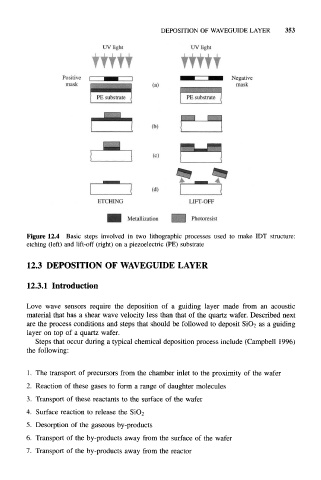
Figure 12.4 Basic steps involved in two lithographic processes used to make IDT structure:
etching (left) and lift-off (right) on a piezoelectric (PE) substrate
12.3 DEPOSITION OF WAVEGUIDE LAYER
12.3.1 Introduction
Love wave sensors require the deposition of a guiding layer made from an acoustic
material that has a shear wave velocity less than that of the quartz wafer. Described next
are the process conditions and steps that should be followed to deposit SiO 2 as a guiding
layer on top of a quartz wafer.
Steps that occur during a typical chemical deposition process include (Campbell 1996)
the following:
1. The transport of precursors from the chamber inlet to the proximity of the wafer
2. Reaction of these gases to form a range of daughter molecules
3. Transport of these reactants to the surface of the wafer
4. Surface reaction to release the SiO 2
5. Desorption of the gaseous by-products
6. Transport of the by-products away from the surface of the wafer
7. Transport of the by-products away from the reactor