
Page 374 - Microsensors, MEMS and Smart Devices - Gardner Varadhan and Awadelkarim
P. 374
354 IDT MICROSENSOR FABRICATION
12.3.2 TMS PECVD Process and Conditions
One of the necessary conditions for the deposition of SiO 2 is that the temperature of
deposition should be as low as possible. This is desirable because higher temperatures
can adversely affect the poling characteristics of quartz (in spite of the fact that quartz
is a naturally piezoelectric material) and because the melting point of the metallisation
layer (aluminum is 650 °C) should not be exceeded.
We should therefore choose SiO 2 that is either sputtered or deposited by plasma-
enhanced chemical vapour deposition (PECVD) from silane gas. The sputtering process
provides better step-coverage than evaporation and far less radiation damage than E-
beam evaporation (Campbell 1996). A simple sputtering system consists of a parallel-plate
plasma reactor in a vacuum chamber and the target material (SiO 2) placed on the electrode
such that it receives the maximum ion flux. An inert gas (at a pressure of 0.1 torr) is usually
used to supply the chamber with high-energy ions that strike the target at high velocities
and dislodge the SiO 2 molecules, which deposit conformal to the wafer (the SAW-IDT
device). The only disadvantage in this process is that on account of the physical nature
of the process, sputtering could also bombard and damage the delicate IDT fingers on the
surface of the quartz. Sputtering can also introduce a variety of contaminants from the
substrate holder because of the physical nature of the process. Hence, sputtering is not
the ideal means of depositing SiO 2, despite the fact that the process can be carried out
under conditions of low temperature.
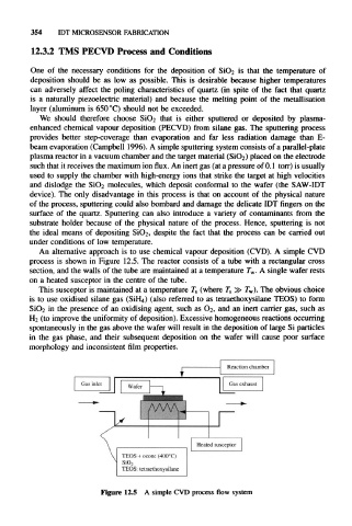
An alternative approach is to use chemical vapour deposition (CVD). A simple CVD
process is shown in Figure 12.5. The reactor consists of a tube with a rectangular cross
section, and the walls of the tube are maintained at a temperature T w. A single wafer rests
on a heated susceptor in the centre of the tube.
This susceptor is maintained at a temperature T s (where T s T w). The obvious choice
is to use oxidised silane gas (SiH 4) (also referred to as tetraethoxysilane TEOS) to form
in the presence of an oxidising agent, such as O2, and an inert carrier gas, such as
SiO 2
H2 (to improve the uniformity of deposition). Excessive homogeneous reactions occurring
spontaneously in the gas above the wafer will result in the deposition of large Si particles
in the gas phase, and their subsequent deposition on the wafer will cause poor surface
morphology and inconsistent film properties.
Figure 12.5 A simple CVD process flow system