
Page 369 - Microsensors, MEMS and Smart Devices - Gardner Varadhan and Awadelkarim
P. 369
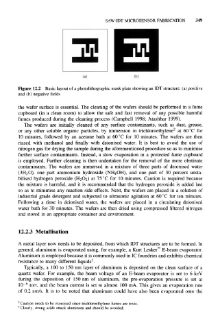
SAW-IDT MICROSENSOR FABRICATION      349


  Figure  12.2  Basic layout of a photolithographic mask plate showing an IDT structure: (a) positive
  and  (b) negative fields


  the  wafer  surface is essential.  The  cleaning  of the wafers should be performed  in  a  fume
  cupboard  (in  a  clean  room)  to  allow  the  safe  and  fast  removal  of  any  possible  harmful
  fumes  produced  during the cleaning  process  (Campbell  1998;  Atashbar  1999).
     The  wafers  are  initially  cleaned  of  any  surface  contaminants,  such  as  dust,  grease,
  or  any  other  soluble  organic  particles,  by  immersion  in  trichloroethylene 2  at  60 °C  for
  10 minutes,  followed  by  an  acetone  bath  at  60 °C  for  10 minutes.  The  wafers  are  then
  rinsed  with  methanol  and  finally  with  deionised  water.  It  is  best  to  avoid  the  use  of
  nitrogen gas for drying the sample during the aforementioned procedure  so as to  minimise
  further  surface  contaminants.  Instead,  a  slow  evaporation  in  a  protected  fume  cupboard
  is  employed.  Further  cleaning  is  then  undertaken for  the  removal  of  the  more  obstinate
  contaminants.  The  wafers  are  immersed  in  a  mixture  of  three  parts  of  deionised  water
  (3H 2O),  one  part  ammonium  hydroxide  (NH 4OH),  and  one  part  of  30  percent  unsta-
  bilised  hydrogen  peroxide  (H 2O 2)  at  75 °C  for  10 minutes.  Caution  is  required  because
  the  mixture  is  harmful,  and  it  is  recommended  that  the  hydrogen  peroxide  is  added  last
  so  as  to  minimise  any  reaction  side  effects.  Next, the  wafers are  placed  in  a  solution of
  industrial  grade  detergent  and  subjected  to  ultrasonic  agitation  at  60 °C for  ten minutes.
  Following  a  rinse  in  deionised  water,  the  wafers  are  placed  in  a  circulating  deionised
  water  bath  for  30 minutes. The  wafers are then dried  using compressed  filtered  nitrogen
  and  stored  in an  appropriate  container  and  environment.


  12.2.3 Metallisation

  A metal layer now needs to be deposited,  from  which IDT structures are to be formed. In
  general, aluminum is evaporated  using, for example,  a Kurt Lesker™  E-beam  evaporator.
  Aluminum is employed because it is commonly used in IC foundries and exhibits chemical
                                3
  resistance  to many different  liquids .
    Typically,  a  100 to  150 nm  layer  of  aluminum is  deposited  on  the  clean  surface of  a
  quartz  wafer.  For  example,  the  beam  voltage  of  an  E-beam  evaporator  is  set  to  6 keV
  during  the  deposition  of  150 nm  of  aluminum,  the  pre-evaporation  pressure  is  set  at
  10 -6  torr,  and the  beam  current is  set to  almost  100 mA.  This  gives  an evaporation  rate
  of  0.2  nm/s.  It  is  to  be  noted  that  aluminum could  have  also  been  evaporated  onto  the

  '  Caution  needs to be exercised since trichloroethylene fumes are toxic.
  3
    Clearly, strong  acids attack  aluminum  and should  be  avoided.