
Page 370 - Microsensors, MEMS and Smart Devices - Gardner Varadhan and Awadelkarim
P. 370
350 IDT MICROSENSOR FABRICATION
device using thermal evaporation instead of using the E-beam technique. The E-beam
technique, however, allows more control over the deposition rate, and the films tend to
be more uniform and to possess fewer stacking faults and dislocations.
E-beam evaporation of aluminum is, indeed, compatible with both the etching and the
lift-off processes used later on.
12.2.4 Photolithography
The photolithography process is conducted in a clean room environment at a constant
temperature of, typically, 25 °C ± 1 °C and at a relative humidity of 40 ± 5 percent.
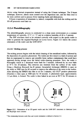
The IDT structures need to be oriented correctly with respect to the quartz wafer in
order to generate the required Rayleigh (or Love) waves. Figure 12.3 shows the correct
4
orientation of the wafer and the SAW-IDTs .
12.2.4.1 Etching process
The etching process begins with the initial cleaning of the metallised wafers, followed by
the deposition of a positive photoresist. The wafers are first rinsed in a bath of acetone and
then in isopropanol to remove any possible loose surface contaminants that could have
appeared during storage since the initial wafer-cleaning procedure. Next, the wafer is
thoroughly rinsed in a deionised water bath for 5 minutes, followed by an oven bake
at 75 °C for 20 minutes. This removes any moisture from the surface of the wafer.
Using a Headway Research Inc.® spinner, hexamethyl disilazane (HMDS) is spun on
the wafer at 3000 rpm for 60 seconds to improve the adhesion of the resist to the wafers.
After allowing the HMDS thin film to sit for 2 minutes, AZ-1512® positive photoresist
(Hoechst) is then spun at 3000 rpm for 30 seconds. A photoresist layer, approximately
1.2 n,m thick, is formed. The wafer is then baked in an oven at 90 °C for 30 minutes to
Major flat Major flat
ST-quartz ST-quartz
Figure 12.3 Orientation of an ST-quartz wafer and the SAW-IDT structures to fabricate Love
and Rayleigh wave sensors
4
The relationship between wafer flats and crystal orientation is defined in Section 4.2.