
Page 81 - Microsensors, MEMS and Smart Devices - Gardner Varadhan and Awadelkarim
P. 81
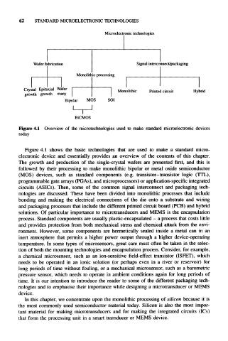
62    STANDARD MICROELECTRONIC   TECHNOLOGIES

                                       Microelectronic technologies


           Wafer  fabrication                      Signal interconnect/packaging
                            Monolithic processing


        Crystal  Epitaxial  Wafer           Monolithic  Printed circuit  Hybrid
        growth  growth  many
                       Bipolar  MOS     SOI
                              I
                           BiCMOS
      Figure 4.1  Overview  of  the  microtechnologies  used  to  make  standard  microelectronic  devices
      today

        Figure  4.1  shows  the  basic  technologies  that  are  used  to  make  a  standard  micro-
      electronic  device  and  essentially  provides  an  overview  of  the  contents  of  this  chapter.
      The  growth  and  production  of  the  single-crystal  wafers  are  presented  first,  and  this  is
      followed  by  their  processing  to  make  monolithic  bipolar  or  metal  oxide  semiconductor
      (MOS)  devices,  such  as  standard  components  (e.g.  transistor—transistor  logic  (TTL),
      programmable gate arrays (PGAs), and microprocessors)  or application-specific  integrated
      circuits  (ASICs).  Then,  some  of  the  common  signal  interconnect  and  packaging  tech
      nologies  are  discussed.  These  have  been  divided  into  monolithic  processes  that include
     bonding  and  making  the  electrical  connections  of  the  die  onto  a  substrate  and  wiring
      and packaging processes  that include the different  printed circuit board (PCB) and hybrid
      solutions.  Of particular importance  to  microtransducers and  MEMS is  the encapsulation
     process. Standard components are usually plastic-encapsulated -  a process  that costs little
      and provides  protection  from  both  mechanical stress  and  chemical attack  from  the envi-
     ronment.  However,  some  components  are  hermetically  sealed  inside  a  metal  can  in  an
      inert  atmosphere  that  permits  a  higher  power  output through a  higher  device-operating
     temperature.  In  some  types  of  microsensors,  great  care  must  often  be taken in  the  selec-
     tion of both the mounting technologies  and encapsulation  process. Consider,  for example,
     a  chemical  microsensor,  such  as  an  ion-sensitive  field-effect  transistor  (ISFET),  which
     needs  to  be  operated  in  an  ionic  solution  (or  perhaps  even  in  a  river  or  reservoir)  for
     long  periods  of time  without fouling,  or a  mechanical  microsensor,  such as a  barometric
     pressure  sensor,  which  needs  to  operate  in  ambient  conditions  again  for  long  periods  of
     time.  It  is  our  intention  to  introduce  the  reader  to  some  of  the  different  packaging  tech-
     nologies  and to emphasise  their  importance  while designing a microtransducer or MEMS
     device.
        In this  chapter,  we concentrate  upon the  monolithic  processing  of silicon because  it is
     the  most  commonly  used  semiconductor  material  today.  Silicon  is  also the  most  impor-
     tant  material  for  making  microtransducers  and  for  making  the  integrated  circuits  (ICs)
     that  form  the  processing  unit  in a smart transducer or MEMS device.