
Page 83 - Microsensors, MEMS and Smart Devices - Gardner Varadhan and Awadelkarim
P. 83
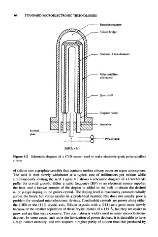
64    STANDARD MICROELECTRONIC TECHNOLOGIES

                                                      Reaction chamber
                                                      Silicon bridge


                                                      Slim rod, 4 mm  diameter


                                                      Polycrystalline
                                                      silicon rod


                                                      Quartz bell


                                                      Graphite holder


                                                      Insulation


                                                         Power input


                                  SiHCl 3  + H 2
     Figure 4.2  Schematic  diagram  of  a  CVD  reactor  used  to  make  electronic-grade  polycrystalline
     silicon


     of  silicon  into a graphite  crucible  that contains  molten  silicon  under an argon  atmosphere.
     The  seed  is  then  slowly  withdrawn  at  a  typical  rate  of  millimeters  per  minute  while
     simultaneously  rotating  the  seed. Figure  4.3  shows a schematic  diagram  of a  Czochralski
     puller  for  crystal  growth.  Either  a  radio  frequency  (RF)  or  an  electrical  source  supplies
     the  heat,  and  a  known  amount  of  the  dopant  is  added  to  the  melt  to  obtain  the  desired
     n-  or P-type doping in the grown crystal.  The doping level is reasonably  constant radially
     across  the  boule  but  varies  axially  in  a  predefined  manner;  this  does  not  usually  pose a
     problem  for standard  microelectronic  devices.  Czochralski  crystals are grown along either
     the  (100)  or  the  (111)  crystal  axis.  Silicon  crystals  with  a (111) axis  grow  more  slowly
     because  of the smaller separation  of these  crystal planes of 4.135  A, but they are easier to
     grow  and are thus less expensive. This orientation is widely used in many  microelectronic
     devices. In some  cases, such as in the fabrication  of power  devices, it is desirable to  have
     a  high carrier  mobility, and  this requires a higher purity  of  silicon than that  produced  by