
Page 88 - Microsensors, MEMS and Smart Devices - Gardner Varadhan and Awadelkarim
P. 88
WAFER PREPARATION
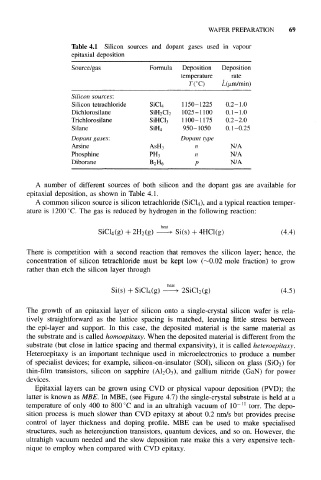
Table 4.1 Silicon sources and dopant gases used in vapour
epitaxial deposition
Source/gas Formula Deposition Deposition
temperature rate
T (ºC) L(um/min)
Silicon sources:
Silicon tetrachloride SiCl 4 1150–1225 0.2-1.0
Dichlorosilane SiH 2Cl 2 1025-1100 0.1-1.0
Trichlorosilane SiHCl 3 1100–1175 0.2-2.0
Si lane SiH 4 950-1050 0.1-0.25
Dopant gases: Dopant type
Arsine AsH 3 n N/A
Phosphine PH 3 n N/A
Diborane B 2H 6 P N/A
A number of different sources of both silicon and the dopant gas are available for
epitaxial deposition, as shown in Table 4.1.
A common silicon source is silicon tetrachloride (SiCl 4), and a typical reaction temper-
ature is 1200°C. The gas is reduced by hydrogen in the following reaction:
SiCl 4(g) + 2H 2(g) Si(s)+4HCl(g) (4.4)
There is competition with a second reaction that removes the silicon layer; hence, the
concentration of silicon tetrachloride must be kept low (~0.02 mole fraction) to grow
rather than etch the silicon layer through
Si(s) + SiCl 4(g) 2SiCl 2(g) (4.5)
The growth of an epitaxial layer of silicon onto a single-crystal silicon wafer is rela-
tively straightforward as the lattice spacing is matched, leaving little stress between
the epi-layer and support. In this case, the deposited material is the same material as
the substrate and is called homoepitaxy. When the deposited material is different from the
substrate (but close in lattice spacing and thermal expansivity), it is called heteroepitaxy.
Heteroepitaxy is an important technique used in microelectronics to produce a number
of specialist devices; for example, silicon-on-insulator (SOI), silicon on glass (SiO 2) for
thin-film transistors, silicon on sapphire (Al 2O 3), and gallium nitride (GaN) for power
devices.
Epitaxial layers can be grown using CVD or physical vapour deposition (PVD); the
latter is known as MBE. In MBE, (see Figure 4.7) the single-crystal substrate is held at a
–11
temperature of only 400 to 800 °C and in an ultrahigh vacuum of 10 torr. The depo-
sition process is much slower than CVD epitaxy at about 0.2 nm/s but provides precise
control of layer thickness and doping profile. MBE can be used to make specialised
structures, such as heterojunction transistors, quantum devices, and so on. However, the
ultrahigh vacuum needed and the slow deposition rate make this a very expensive tech-
nique to employ when compared with CVD epitaxy.