Page 92 - Microsensors, MEMS and Smart Devices - Gardner Varadhan and Awadelkarim
P. 92
MONOLITHIC PROCESSING     73

     conductivity.  In addition, SOI technology offers  extremely low unwanted parasitic  effects
     and  excellent  isolation  between devices  (see  Section  4.3.5).


     4.3.1  Bipolar  Processing

     The  bipolar  process  has  evolved  over  many  years,  as  has  its  so-called  standard  process.
     Clearly,  this is  an important issue and  the integration  of a microsensor,  or  microactuator,
     will  depend  on  the  exact  details  of  the  process  that  is  employed.  As  stated  earlier,  the
     possible  approaches  to microsensors  and MEMS  integration  and the  problems  associated
     with compliance  to a standard process  are both  discussed  in some  detail  in later chapters.
       This  section  presents  what  may  be  regarded  as  the  standard  bipolar  process,  which
     employs  an  epi-layer  to  make  the  two  most  important  types of  bipolar  components; that
     is,  vertical  and lateral  transistors. Bipolar  n-p-n  transistors are the most commonly  used
     components  in  circuit  design  as  both  amplifiers  and  switches  because  of  their  superior
     characteristics compared  with p-n-p  transistors.  Let us now consider  in detail the process
     steps  required  to  make  a  vertical  n-p-n  and  lateral  p-n-p  transistors.  A  similar  process
     can be defined  to make vertical p-n-p  transistors or the simpler substrate p-n-p  transistors
     with  slightly different  device  characteristics.


       Worked  Example   E4.1:  Vertical and Lateral Bipolar Transistors
       The  standard bipolar  process  begins  by  taking  a  p-type  substrate (i.e. single-crystal
                                       2
       silicon  wafer)  with  the topside polished . A buried n-layer is  formed  within  the  p-type
       substrate  by  first  growing an  oxide  layer. The  oxide is  usually  grown  in  an oxidation
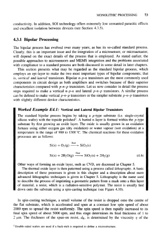
       furnace  using  either oxygen  gas  (dry oxidation) or  water  vapour  (wet oxidation)  at  a
       temperature  in  the  range  of  900  to  1300 °C. The  chemical  reactions  for  these oxidation
       processes  are as  follows:


                         Si(s) +  2H 2O(g)  SiO 2(s) + 2H 2(g)           (4.6)


       Other  ways  of  forming  an oxide layer, such  as CVD, are discussed in Chapter 5.
          The thermal oxide  layer is then patterned using a process  called  lithography. A  basic
       description  of  these  processes  is  given  in  this  chapter and  a  description  about  more
       advanced  lithographic techniques is  given  in  Chapter 5.  Lithography is  the  name used
       to describe the  process of imprinting a geometric pattern from  a mask onto a thin layer
       of  material, a  resist, which  is  a  radiation-sensitive polymer.  The  resist  is  usually  laid
       down  onto the  substrate using  a spin-casting  technique  (see Figure 4.10).


       In  spin-casting  technique,  a  small  volume  of  the  resist  is  dropped  onto  the  centre of
     the  flat  substrate,  which  is  accelerated  and  spun  at  a  constant  low  spin  speed  of  about
     2000  rpm  to  spread  the  resist  uniformly. The  spin  speed  is  then  rapidly  increased  to  its
     final  spin  speed  of  about  5000 rpm,  and  this  stage  determines  its  final  thickness  of  1 to
     2  um.  The  thickness  of  the  spun-on resist,  d R,  is  determined  by  the  viscosity  77  of  the
     2
      Double-sided wafers  are used if a back-etch is required to define  a microstructure.

