
Page 90 - Microsensors, MEMS and Smart Devices - Gardner Varadhan and Awadelkarim
P. 90
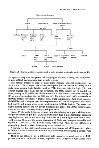
MONOLITHIC PROCESSING     71

                             Silicon microtechnologies


                    Bipolar     Bipolar/MOS  Metal oxide semiconductor
                                                   (MOS)
                                 BiC MOS

         Analogue  Transistor-  Integrated  Emitter  RF  Silicon on
                transistor  injection  coupled  Bulk     insulator
                logic   logic    logic        processes  (SOI)
                (TTL)   (IIL)   (ECL)


                                                          CMOS
                                                            I

                 nMOS      CMOS      CMOS    Sapphire  Implanted  Wafer  Unibond
                           metal     polysilicon    oxygen  bonding
                           gate      gate


                          P-well    N-well  Twin (tub) well

      Figure  4.8  Common  silicon  processes  used to make  standard semiconductor  devices  and ICs

     analogue  circuitry  with  low-power  switching  digital  circuitry. Clearly,  this  dual  process
     is  more  difficult  and  expensive  than  a single  process.
       The  bipolar  process  is  used  to  make  many  standard  analogue  components  (see
     Section 4.3.1),  for  example,  p-n  diodes  and  bipolar junction  transistors  (BJTs),  and  to
     make  some  popular  logic  families,  such  as  TTL, integrated  injection  logic  (IIL),  and
     emitter  coupled  logic  (ECL)  for  fast  switching.  The  MOS  process  can  be  divided  into
     those  creating  an  IC  within  the  silicon  wafer  (i.e. a bulk  process)  and  those  creating  an
     IC  on  top  of  an  insulator (i.e. an  SOI  process).  The  n-type  metal  oxide  semiconductor
     (nMOS)  process  only  makes  n-channel  metal  oxide  semiconductor  field-effect  transistor
     (MOSFETs)  and  is  simpler  than  the  complementary  MOS  (CMOS)  process  that  makes
     both  nMOS  and  p-type  metal  oxide  semiconductor  (pMOS)  devices.  The  lower  cost,
     higher  packing  density,  and  low power  dissipation  per  gate  of  the  CMOS  process  makes
     it  one  of the  most  commonly  used  technologies  today.
       Figure  4.9 shows the difference  between the main technologies  in gate-switching  speed
     and  power dissipation  per gate.  GaAs has traditionally  been  a niche technology  producing
     very  high-speed  devices  and  switching  circuits  but  at  a  much  higher  cost  from  a  lower
     yield  process.  However,  the  power  dissipation  of  GaAs  does  compare  favorably  with
     bipolar  TTL  and  ECL, and, in  some  cases,  with  CMOS  when  the  cost  difference  is
     diminishing;  therefore,  GaAs  is  becoming  more  competitive.
       A  summary  of the relative  performances  of basic  bipolar  and  MOS  processes  is given
     in Table 4.2. Most of the devices available for circuit design are described  in the  following
     two  sections.
       There  is  the  option  to  use  a  polysilicon  gate  instead  of  a  metal  gate  in  a  CMOS
     process  with  an  N-  or  P-well  (or  both)  implanted into  a  p-type  or  n-type  silicon  wafer