
Page 93 - Microsensors, MEMS and Smart Devices - Gardner Varadhan and Awadelkarim
P. 93
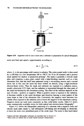
74    STANDARD MICROELECTRONIC   TECHNOLOGIES


                                             Pipette


                                                  Liquid

                                Spin
                                                 Wafer


                                               Motor


                                     Vacuum line

      Figure  4.10  Apparatus used to cast a resist onto a substrate in preparation  for optical  lithography

      resist and final spin  speed  v  approximately  according  to


                                    ^R  =  -?=  x  /sc                      (4.7)


     where  f sc  is the percentage  solid content  in solution.  The resist-coated wafer is then cured
     by  a  soft-bake  at  a  low  temperature  (80  to  100°C  for  10 to  20 minutes)  and  a  process
                                             3
     mask  applied  for  shadow  or  projection  printing .  The  mask  is  generally  a reticule  mask
     plate  and  comprises  a  glass  plate  coated  with  a  light-blocking  material,  such  as  a  thin
     chromium  film,  that  has  itself  been  patterned  using a  wet-etching  process  and a  second
     resist,  but  in  this  case  the  resist  has  been  written  on  directly  using  a  high-resolution
     electron-beam  writer.  Then  the  mask  and  substrate  are  exposed  to  a  radiation  source,
     usually  ultraviolet  (UV)  light,  and the  radiation  is  transmitted  through  the  clear parts  of
     the mask but blocked  by the chromium coating. The effect  of the radiation depends on the
     type  of resist  -  positive  or negative.  When a positive  resist  is exposed  to the radiation,
     it  becomes  soluble  in  the  resist  developer  and  dissolves  leaving  a  resist  pattern  of  the
     same  shape  as  that  of  the  chromium  film.  Conversely,  the  negative  resist  becomes  less
     soluble when exposed  to the radiation and so leaves the negative of the chromium coating.
     Negative  resists  are  used  more  commonly  as  they  yield  better  results.  Table 4.3  shows
                                                                           4
     some  commercially  available  resists for both  optical  and electron-beam  lithography .
        Figure  4.11  shows  the lithographic  patterning  of a substrate  with a negative  resist  and
     chrome  mask  plate  (mask  1), and  subsequent  soft-baking  and  developing  in  chemicals,
     to  leave the  resist  over  predefined  parts  of  the  oxide  layer. The  resist  is then hard-baked

     3
       Optical and other lithographic techniques are described  later in Section  5.3.
     4
       These terms are defined  later on under bipolar transistor characteristics.