
Page 89 - Microsensors, MEMS and Smart Devices - Gardner Varadhan and Awadelkarim
P. 89
70 STANDARD MICROELECTRONIC TECHNOLOGIES
Main shutter
Rotating substrate holder
Effusion oven
Ga
Sample exchange
Dopant load lock
Effusion oven shutters
To variable speed
motor and substrate
heater only
GaAs Monocrystal substrate
Molecular beams
Ga
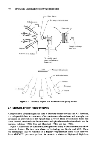
Figure 4.7 Schematic diagram of a molecular beam epitaxy reactor
4.3 MONOLITHIC PROCESSING
A large number of technologies are used to fabricate discrete devices and ICs; therefore,
it is only possible here to cover some of the most commonly used ones and to simply give
the reader an appreciation of the typical steps involved. There are numerous books that
cover, in detail, semiconductor fabrication technologies (Interested readers should see, for
example, Colclaser (1980), Gise and Blanchard (1986), and Sze (1985)).
Figure 4.8 illustrates the common technologies used today to fabricate standard micro-
electronic devices. The two main classes of technology are bipolar and MOS. These
two technologies can be combined in a bipolar complementary metal oxide semicon-
ductor (BiCMOS) process to produce, for example, a mixture of high-speed, high-drive