
Page 94 - Microsensors, MEMS and Smart Devices - Gardner Varadhan and Awadelkarim
P. 94
MONOLITHIC PROCESSING 75
Table 4.3 Some commercially available resists
Resist Lithography Type
Kodak 747 Optical Negative
AZ-1350J Optical Negative
Shippley S-1813 Optical Negative
PR 102 Optical Positive
COP E-beam and X-ray Negative
PMMA E-beam and X-ray Positive
PBS E-beam and X-ray Positive
Exposing radiation
Glass
Mask
Chromium (80 nm)
An image-forming system may occupy
a portion of this space
Resist
Oxide or mulptiple layers of device
Wafer Wafer substrate
Resist
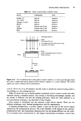
Figure 4.11 Use of radiation and a mask plate to create windows in a resist layer through which
the oxide is etched and arsenic-doped to form buried n-regions in a p-type substrate. The buried
regions are used to increase device performance
(110 to 130 °C for 10 to 20 minutes) and the oxide is selectively removed using either a
wet-etching or a dry-etching process.
Table 4.4 shows the wet or liquid etchants commonly used to remove oxides and other
materials during a standard process. Dry etching is becoming increasingly popular, and
the details of different wet and dry etching processes, which are often referred to as
micromachining techniques, are described in this Chapter.
Next, arsenic is introduced into the exposed p-type silicon regions. There are two
different techniques used: thermal predeposition and ion implantation.
In thermal predeposition, a powder, liquid, or gas can be used as the source dopant
material for the predeposition process. The solid solubility of the dopant in the material,
predeposition time, and temperature determine how far the dopant diffuses into the wafer.
For a constant source concentration C s, the dopant concentration at distance x and at time